SFH6319T Vishay, SFH6319T Datasheet - Page 4
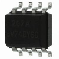
SFH6319T
Manufacturer Part Number
SFH6319T
Description
OPTOCOUPLER 100KBD 3500% 8SOIC
Manufacturer
Vishay
Specifications of SFH6319T
No. Of Channels
1
Input Current
1.6mA
Output Voltage
18V
Opto Case Style
SOIC
No. Of Pins
8
Isolation Voltage
4kV
Voltage - Isolation
4000Vrms
Number Of Channels
1, Unidirectional
Current - Output / Channel
60mA
Propagation Delay High - Low @ If
600ns @ 12mA
Current - Dc Forward (if)
20mA
Input Type
DC
Output Type
Logic
Mounting Type
Surface Mount
Package / Case
8-SOIC (3.9mm Width)
Current Transfer Ratio (max)
3500% @ 500µA
Current Transfer Ratio (min)
400% @ 500µA
Approval Bodies
UL, CSA
Current Transfer Ratio Min
500%
Current Transfer
RoHS Compliant
Optocoupler Output Type
Photodarlington
Propagation Delay Low-high
60µs
Rohs Compliant
Yes
Lead Free Status / RoHS Status
Lead free / RoHS Compliant
Voltage - Output
-
Vce Saturation (max)
-
Lead Free Status / RoHS Status
Lead free / RoHS Compliant, Lead free / RoHS Compliant
Available stocks
Company
Part Number
Manufacturer
Quantity
Price
Company:

Part Number:
SFH6319T
Manufacturer:
SIEMENS
Quantity:
5 510
Company:
Part Number:
SFH6319T
Manufacturer:
INFINEON
Quantity:
5 510
Part Number:
SFH6319T
Manufacturer:
VISHAY/威世
Quantity:
20 000


SFH6318T/ SFH6319T
Vishay Semiconductors
Switching Characteristics
T
Common Mode Transient Immunity
1. DC current transfer ratio is defined as the ratio of output collector current, I
2. Pin 7 open.
3. Device considered a two-terminal device: pins 1, 2, 3 and 4 shorted together and pins 5, 6, 7 and 8 shorted together.
4. Using a resistor between pin 5 and 7 will decrease gain and delay time.
5. Common mode transient immunity in logic high level is the maximum tolerable (positive) dV
mode pulse, V
level is the maximum tolerable (negative) dV
will remain in a logic low state (i.e.V
6. In applications where dv/dt may exceed 50,000 V/µs (such as state discharge) a series resistor, R
from destructively high surge currents. The recommended value is Refer to Figure 2.
R
www.vishay.com
4
Propagation delay time to logic
low at output
Propagation delay time to logic
low at output, see notes 2 and 4
Propagation delay time to logic
low at output
Propagation delay time to logic
high at output
Propagation delay time to logic
high at output, see notes 2 and 4
Propagation delay time to logic
high at output
Common mode transient
immunity at logic high level
output, see notes 5 and 6
Common mode transient
immunity at logic low level
output, see notes 5 and 6
amb
CC
isfh6318t_01
10% Duty Cycl
1/f<100 µs
I F = Monitor
Pulse
Generator
Z O = 50 Ω
t r = 5 ns
≅ [(IV)/0.15 I
= 25 °C
Parameter
Parameter
CM
R m
I F
, to assure that the output will remain in a logic high state (i.e. V
F
(mA)] kΩ.
1
2
3
4
I
I
I
I
I
I
I
V
I
V
F
F
F
F
F
F
F
F
O
CM
CM
= 1.6 mA, R
= 0.5 mA, R
= 12 mA, R
= 1.6 mA, R
= 0.5 mA, R
= 12 mA, R
= 0 mA, R
= 1.6 mA, R
< 0.8 V).
= 10 V
= 10 V
Test condition
Test condition
8
7
6
5
cm
P-P
P-P
L
/dt on the trailing edge of the common mode pulse signal, V
L
L
= 2.2 kΩ,
L
L
L
L
L
= 270 Ω
= 270 Ω
= 2.2 kΩ
= 4.7 kΩ
= 2.2 kΩ
= 4.7 kΩ
= 2.2 kΩ,
0.1 µ F
Figure 1. Switching Test Circuit
R L
C L =15pF
+5 V
V O
SFH6318T
SFH6319T
SFH6319T
SFH6318T
SFH6319T
SFH6319T
Symbol
I CM
I CM
(Non-Saturated
Part
Response)
(Saturated
H
L
Response)
V O
O
I
I F
V O
I
0
, to the forward LED input current, I
t PHL
O
> 2.0 V) common mode transient immunity in logic low
Symbol
Min
t
t
t
t
t
t
PHL
PHL
PHL
PLH
PLH
PLH
90%
10%
1.5 V
t f
cm
/dt on the leading edge of the common
Min
t PLH
Typ.
1K
1K
CC
10%
should be included to protect I
90%
CM
Typ.
2.0
6.0
0.6
2.0
4.0
1.5
1.5 V
, to assure that the output
Document Number 83678
t r
Max
F
V OL
times 100 %
5 V
Rev. 1.4, 26-Oct-04
5 V
Max
1.0
7.0
10
25
35
60
V/µs
V/µs
Unit
Unit
µs
µs
µs
µs
µs
µs
C
Related parts for SFH6319T
Image
Part Number
Description
Manufacturer
Datasheet
Request
R

Part Number:
Description:
357-036-542-201 CARDEDGE 36POS DL .156 BLK LOPRO
Manufacturer:
Vishay
Datasheet:
Part Number:
Description:
357-036-542-201 CARDEDGE 36POS DL .156 BLK LOPRO
Manufacturer:
Vishay
Datasheet:
Part Number:
Description:
357-036-542-201 CARDEDGE 36POS DL .156 BLK LOPRO
Manufacturer:
Vishay
Datasheet:
Part Number:
Description:
357-036-542-201 CARDEDGE 36POS DL .156 BLK LOPRO
Manufacturer:
Vishay
Datasheet:
Part Number:
Description:
357-036-542-201 CARDEDGE 36POS DL .156 BLK LOPRO
Manufacturer:
Vishay
Datasheet:
Part Number:
Description:
357-036-542-201 CARDEDGE 36POS DL .156 BLK LOPRO
Manufacturer:
Vishay
Datasheet:
Part Number:
Description:
357-036-542-201 CARDEDGE 36POS DL .156 BLK LOPRO
Manufacturer:
Vishay
Datasheet:
Part Number:
Description:
357-036-542-201 CARDEDGE 36POS DL .156 BLK LOPRO
Manufacturer:
Vishay
Datasheet:
Part Number:
Description:
357-036-542-201 CARDEDGE 36POS DL .156 BLK LOPRO
Manufacturer:
Vishay
Datasheet:
Part Number:
Description:
357-036-542-201 CARDEDGE 36POS DL .156 BLK LOPRO
Manufacturer:
Vishay
Datasheet:
Part Number:
Description:
357-036-542-201 CARDEDGE 36POS DL .156 BLK LOPRO
Manufacturer:
Vishay
Datasheet:
Part Number:
Description:
357-036-542-201 CARDEDGE 36POS DL .156 BLK LOPRO
Manufacturer:
Vishay
Datasheet:
Part Number:
Description:
357-036-542-201 CARDEDGE 36POS DL .156 BLK LOPRO
Manufacturer:
Vishay
Datasheet:
Part Number:
Description:
357-036-542-201 CARDEDGE 36POS DL .156 BLK LOPRO
Manufacturer:
Vishay
Datasheet:
Part Number:
Description:
357-036-542-201 CARDEDGE 36POS DL .156 BLK LOPRO
Manufacturer:
Vishay
Datasheet: