TLP621-4(F) Toshiba, TLP621-4(F) Datasheet
TLP621-4(F)
Specifications of TLP621-4(F)


Related parts for TLP621-4(F)

TLP621-4(F) Summary of contents
Page 1
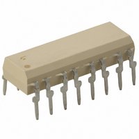
... The TOSHIBA TLP621, −2 and −4 consists of a photo−transistor optically coupled to a gallium arsenide infrared emitting diode. The TLP621−2 offers two isolated channels in an eight lead plastic DIP, which the TLP621−4 provides four isolated channels in a sixteen plastic DIP. • ...
Page 2
... TLP621 Rank GR Rank BL Rank GB (None) TLP621−2 TLP621−4 Rank GB *1: Ex. rank GB: TLP621 (GB) (Note) Application type name for certification test, please use standard product type name, i.e. TLP621 (GB): TLP621 TLP621−2 (GB): TLP621−2 Made In Japan UL recognized E67349 BSI approved 6508, 7445 ...
Page 3
... When a EN 60747-5-2 approved type is needed, please designate the “Option (D4)” 7.62 mm pich standard type • Creepage distance : 6.4 mm (min.) Clearance : 6.4 mm (min.) Insulation thickness : 0.4 mm (min.) TLP621,TLP621−2,TLP621− 10.16 mm pich (LF2) type 8.0 mm (min) 8.0 mm (min) 0.4 mm (min) 3 2007-10-01 ...
Page 4
... T BV 5000 (AC, 1min., R.H.≤ 60%) S Symbol Min. Typ. V ― ― ― −25 T ― opr 4 Unit TLP621−2 TLP621− −0.5 (Ta = 25°C) mA /° −0.7 mW /°C V ° 100 mW −1.0 mW /°C °C °C °C °C 150 mW −1.5 mW /°C V rms Max. ...
Page 5
... (sat 0.2 mA (Ta = 25°C) Symbol Test Condition MHz 500 AC, 1 minute BV AC, 1 second, in oil S DC, 1 minute, in oil 5 TLP621,TLP621−2,TLP621−4 Min. Typ. Max. 1.0 1.15 1.3 — — 10 — 30 — 55 — — 7 — — — 10 100 — — 10 — MIn. Typ. ...
Page 6
... Fig. 1 Switching time test circuit I F (Ta = 25°C) Symbol Test Condition 100Ω off 1.9 kΩ (Fig. OFF TLP621,TLP621−2,TLP621−4 Min. Typ. Max. — 2 — — 3 — — 3 — — 3 — — 2 — — 15 — — 25 — 4.5V 0. OFF 2007-10-01 Unit μs μs ...
Page 7
... Pulse width ≤ 100μ 25°C 1000 500 300 100 Duty cycle ratio DR TLP621,TLP621−2,TLP621−4 TLP621-2 TLP621-4 100 100 120 -20 0 Ambient temperature Ta (°C) TLP621-2 TLP621-4 120 100 100 120 -20 0 Ambient temperature Ta (°C) TLP621-2 TLP621-4 3000 1000 500 300 100 – ...
Page 8
... Pulse forward voltage – 25°C 60 50mA 30mA 20mA 40 15mA P C (MAX.) 10mA 5mA Collector-emitter voltage V CE TLP621,TLP621−2,TLP621−4 -2.8 -2.4 -2.0 -1.6 -1.2 -0.8 -0.4 0.1 1.4 1.6 0 2.0 2.4 (V) Ambient temperature 0.2 0 (V) Collector-emitter voltage V 8 Δ ...
Page 9
... F I – 100 25mA 50 30 10mA 5mA 1mA 1 0 0.5mA 0.3 0.1 - Ambient temperature T (°C) a TLP621,TLP621−2,TLP621−4 500 300 Sample A 100 Sample 0.3 1 Forward current I 100 0. 5mA 1mA 0.16 0.12 0.08 0.04 0 -20 Ambient temperature T 1000 Ta = 25° 16mA 500 ...
Page 10
... Please use Product in compliance with all applicable laws and regulations that regulate the inclusion or use of controlled substances, including without limitation, the EU RoHS Directive. TOSHIBA assumes no liability for damages or losses occurring as a result of noncompliance with applicable laws and regulations. TLP621,TLP621−2,TLP621−4 10 2007-10-01 ...