C-51849NFJ-SLW-ADN Optrex America Inc, C-51849NFJ-SLW-ADN Datasheet - Page 7
C-51849NFJ-SLW-ADN
Manufacturer Part Number
C-51849NFJ-SLW-ADN
Description
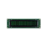
LCD MOD CHAR 40X4 WHT TRANSFLECT
Manufacturer
Optrex America Inc
Series
C-51849r
Datasheets
1.C-51848NFJ-SLW-ADN.pdf
(2 pages)
2.C-51849NFJ-SLW-ADN.pdf
(1 pages)
3.C-51849NFJ-SLW-ADN.pdf
(17 pages)
Specifications of C-51849NFJ-SLW-ADN
Display Mode
Transflective
Display Type
STN - Super-Twisted Nematic
Number Of Digits/alpha
160
Outline L X W X H
190.00mm x 54.00mm x 14.60mm
Viewing Area
147.00mm L x 29.50mm W
Backlight
LED - White
Display Format
40 x 4
Character Format
5 x 8 Dots
Voltage - Supply
5.0V
Interface
Parallel
Operating Temperature
-20°C ~ 70°C
Character Count X Line
40 x 4
Module Size (w X H X T)
190 mm x 54 mm x 14.6 mm
Fluid Type
FSTN
Background Color
White
Backlight Type
LED White
Lead Free Status / RoHS Status
Lead free / RoHS Compliant
Dot Size
-
Character Size
-
Lead Free Status / Rohs Status
Lead free / RoHS Compliant
Other names
73-1255
Available stocks
Company
Part Number
Manufacturer
Quantity
Price
Company:

Part Number:
C-51849NFJ-SLW-ADN
Manufacturer:
TI
Quantity:
3 060


Recommended
Contrast Ratio
Viewing Angle
Response
C-51849NFJ-SLW-ADN (AD) No. 2005-0246
3. Optical Specifications
Note 1 : Voltage (Applied actual waveform to LCD Module) for the best contrast. The range of
Note 1 :Contrast ratio is definded as follows.(CR = L
Note 2 :The time that the luminance level reaches 90% of the saturation level from 0%
Note 3 :The time that the luminance level reaches 10% of the saturation level from 100%
Note 4 :Definition of Driving Voltage V
3.1. LCD Driving Voltage
3.2. Optical Characteristics
LCD Driving Voltage
Time
Parameter
Parameter
minimum and maximum shows tolerance of the operating voltage. The specified contrast
ratio and response time are not guaranteed over the entire range.
L
L
Measuring Spot :3.0mm
when ON signal is applied.
when OFF signal is applied.
Assuming that the typical driving waveforms shown below are applied to the LCD
Panel at 1/A Duty - 1/B Bias (A: Duty Number, B: Bias Number). Driving voltage
V
Vth1: The voltage V
Vth2: The voltage V
ON
OFF
OD
Rise Note 2
Decay Note 3
V
is definded as follows.
: Luminance of the ON segments
: Luminance of the OFF segments
OD
Vo-p
luminance at the segment which the ON signal is applied to.
luminance at the segment which the OFF signal is applied to.
= (Vth1+Vth2) / 2
Note 1
Note 1
1/( f
( ON SIGNAL )
F
A )
O-P
O-P
V
Symbol
Symbol
CC
T
T
CR
OFF
that should provide 70% of the saturation level in the
that should provide 20% of the saturation level in the
ON
-V
EE
OD
Ta=25 C, 1/16 Duty, 1/4 Bias, V
Conditions
Conditions
Ta= -20 C
Ta=25 C
Ta=70 C
= 0 , =-
-
-
OFF
OPTREX CORPORATION
/ L
ON
)
1 /f
( OFF SIGNAL )
Shown in 3.3
F
Min.
Min.
4.4
4.2
-
-
-
-
OD
=4.8V (Note 4), = 0 , =-
( B-2 ) Vo-p/B
Typ.
Typ.
130
4.8
5.0
80
-
-
Max.
Max.
160
200
5.2
5.2
-
-
Page 7/17
Units
Units
ms
ms
V
V
V
Related parts for C-51849NFJ-SLW-ADN
Image
Part Number
Description
Manufacturer
Datasheet
Request
R

Part Number:
Description:
LCD 6.5" TFT MOD 640X480 VGA
Manufacturer:
Optrex America Inc

Part Number:
Description:
LCD Graphic Display Modules & Accessories OPTREX
Manufacturer:
Optrex America Inc

Part Number:
Description:
LCD MODULE 16X2 CHARACTER
Manufacturer:
Optrex America Inc
Datasheet:

Part Number:
Description:
LCD MOD CHAR 20X2 TRANSMISSIVE
Manufacturer:
Optrex America Inc
Datasheet:

Part Number:
Description:
LCD MODULE 16X1 W/LED BACKLIGHT
Manufacturer:
Optrex America Inc
Datasheet:

Part Number:
Description:
LCD MOD CHAR 16X2 WHT TRANSFLECT
Manufacturer:
Optrex America Inc
Datasheet:

Part Number:
Description:
LCD MODULE 20X2 GREEN CHARACTER
Manufacturer:
Optrex America Inc
Datasheet:

Part Number:
Description:
LCD MODULE 20X2 BLUE CHARACTER
Manufacturer:
Optrex America Inc
Datasheet:

Part Number:
Description:
LCD MODULE 20X2 WHITE CHARACTER
Manufacturer:
Optrex America Inc
Datasheet:
Part Number:
Description:
LCD MOD 16X2 CHARAC TRANS W/LED
Manufacturer:
Optrex America Inc
Datasheet:

Part Number:
Description:
LCD MOD CHAR 20X4 WHT TRANSFLECT
Manufacturer:
Optrex America Inc
Datasheet:

Part Number:
Description:
LCD MODULE 16X2 HI CONT STD LED
Manufacturer:
Optrex America Inc

Part Number:
Description:
LCD MOD CHAR 20X4 WHT TRANSMISS
Manufacturer:
Optrex America Inc
Datasheet:

Part Number:
Description:
LCD MOD CHAR 16X2 WHT TRANSMISS
Manufacturer:
Optrex America Inc
Datasheet:

Part Number:
Description:
LCD MOD 16X2 CHARAC TRANS W/LED
Manufacturer:
Optrex America Inc
Datasheet: