SCE5781 OSRAM Opto Semiconductors Inc, SCE5781 Datasheet - Page 7
SCE5781
Manufacturer Part Number
SCE5781
Description
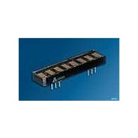
DISPLAY 8CHAR .180" 5X7 SER YLW
Manufacturer
OSRAM Opto Semiconductors Inc
Series
Intelligent Display®r
Datasheet
1.SCE5782.pdf
(15 pages)
Specifications of SCE5781
Millicandela Rating
110µcd
Size / Dimension
1.69" L x 0.45" W x 0.21" H (42.93mm x 11.43mm x 5.33mm)
Color
Yellow
Configuration
5 x 7
Number Of Digits
8
Character Size
0.18 in
Illumination Color
Yellow
Wavelength
585 nm
Maximum Operating Temperature
+ 85 C
Minimum Operating Temperature
- 40 C
Luminous Intensity
110 ucd
Viewing Area (w X H)
2.54 mm x 4.57 mm
Display Type
5 x 7 Dot Matrix
Lead Free Status / RoHS Status
Lead free / RoHS Compliant
Voltage - Forward (vf) Typ
-
Internal Connection
-
Lead Free Status / Rohs Status
Details
Other names
Q68000A9101
Available stocks
Company
Part Number
Manufacturer
Quantity
Price

Part Number:
SCE5781
Manufacturer:
OSRAM/欧司朗
Quantity:
20 000


Block Diagram
Operation of the SCE578X
The SCE578X display consists of two CMOS ICs containing con-
trol logic and drivers for eight 5 x 7 characters. The first IC controls
characters 0 through 3 and the second IC controls characters 4
through 7. These components are assembled in a compact plastic
package.
Individual LED dot addressability allows the user great freedom in
creating special characters or mini-icons.
The serial data interface provides a highly efficient interconnection
between the display and the mother board. The SCE578X requires
a minimum three input lines as compared to fourteen for an equiva-
lent eight character parallel input part.
The on-board CMOS IC is the electronic heart of the display. Each
IC accepts serially formatted data, which is stored in the internal
RAM. The IC accepts data based on the character address
selected. The first IC is selected when addressing characters 0
through 3, the second IC is selected when addressing characters 4
though 7, and both ICs are selected when the Control Word is
addressed.
Asynchronously the RAM is read by the character multiplexer at a
strobe rate that results in a flicker free display. The Block Diagram
shows the three functional areas of the IC. These include: the input
serial data register and control logic, a 140 bit two port RAM, and
an internal multiplexer/display driver. The second IC is identical
except characters 4 though 7 are driven.
The following explains how to format the serial data to be loaded
into the display. The user supplies a string of bit mapped decoded
2006-01-23
CLKSEL
CLK I/O
RESET
SD CLK
SDATA
LOAD
IC 1
Oscillator
Register
Serial
Data
& Timing Logic
Counter Chain
IC 2 controls characters 4 to 7
The second IC has the same
Function diagram as IC 1
Control Word Logic
Display Multiplexer
X Address Decode
Word Register
VDIM Controls
3-bit Address
140 bit RAM
Read 7 x 20
6-bit Control
Write 28 x 5
7
Register
characters. The contents of this string is shown in Figure „Loading
Serial Character Data“ a
ter Data“ b
bit words. The first word encodes the display character location and
the succeeding seven bytes are row data. The row data represents
the status (On, Off) of individual column LEDs. Figure „Loading
Serial Character Data“ c
matted to represent Character Address, or Column Data.
Figure „Loading Serial Character Data“ d
sequence for loading the bytes of data. Bringing the LOAD line low
enables the serial register to accept data. The shift action occurs
on the low to high transition of the serial data clock (SDCLK). The
least significant bit (D0) is loaded first. After eight clock pulses the
LOAD line is brought high. With this transition the OPCODE is
decoded. The decoded OPCODE directs D4–D0 to be latched in
the Character Address register, stored in the RAM as Column
data, or latched in the Control Word register. The control IC
requires a minimum 600 ns delay between successive byte loads.
As indicated in Figure „Loading Serial Character Data“ a
a total of 512 bits of data are required to load all eight characters
into the display.
The Character Address Register selects the character address that
the row and column data will be written to. See Table „Load Char-
acter Adress“
loading the Character Address Register, the next seven bytes load
the column data, one row at a time, starting with row 0 (top row)
and ending with row 6 (bottom row). Each character address has a
7 x 5 bit User RAM formatted as seven rows, each containing five
MUX
Rate
(
page 8
(
page 9
Column
Drivers
Digits
0 to 3
Row Decoder
)
& Driver
shows that each character consist of eight 8
)
for opcode and character addressing. After
(
(
page 8
page 8
)
)
. Figure „Loading Serial Charac-
shows that each 8 bit word is for-
0
4
Characters
Characters
4 - 5 x 7
4 - 5 x 7
5
1 2
(
6
page 8
IDBD5071
IC 2
3
7
)
SCE5780
shows the
(
page 8
)
,
Related parts for SCE5781
Image
Part Number
Description
Manufacturer
Datasheet
Request
R

Part Number:
Description:
INTELLIGENT DISP 4CHAR 5X7 HERED
Manufacturer:
OSRAM Opto Semiconductors Inc
Datasheet:

Part Number:
Description:
DISPLAY 8DIGIT CERAMIC GREEN
Manufacturer:
OSRAM Opto Semiconductors Inc
Datasheet:

Part Number:
Description:
EMITTER IR 950NM 5MM SMD RADIAL
Manufacturer:
OSRAM Opto Semiconductors Inc
Datasheet:

Part Number:
Description:
LED TOPLED GREEN 570NM 2-PLCC
Manufacturer:
OSRAM Opto Semiconductors Inc
Datasheet:

Part Number:
Description:
INTERRUPTER RELFECT W/FILTR SMD
Manufacturer:
OSRAM Opto Semiconductors Inc
Datasheet:

Part Number:
Description:
LED Displays 5x7 Green 0.145 , 4-CHARACTER
Manufacturer:
OSRAM Opto Semiconductors Inc
Datasheet:

Part Number:
Description:
Q65110A4321_SIDELED PURE GREEN EOL150407
Manufacturer:
OSRAM Opto Semiconductors Inc
Datasheet:
Part Number:
Description:
Q65110A1202_RO DETECTOR 3/5MM_TR_RO
Manufacturer:
OSRAM Opto Semiconductors Inc
Datasheet:

Part Number:
Description:
PHOTODIODE 900NM 3MM W/FILTER
Manufacturer:
OSRAM Opto Semiconductors Inc
Datasheet:
Part Number:
Description:
INTELLIGENT DISP 4CHAR 5X7 HERED
Manufacturer:
OSRAM Opto Semiconductors Inc
Datasheet:
Part Number:
Description:
LED TOPLED GREEN 570NM 2-PLCC
Manufacturer:
OSRAM Opto Semiconductors Inc
Datasheet:
Part Number:
Description:
PHOTODIODE 900NM 3MM W/FILTER
Manufacturer:
OSRAM Opto Semiconductors Inc
Datasheet:

Part Number:
Description:
PHOTODIODE 850NM THRU-HOLE
Manufacturer:
OSRAM Opto Semiconductors Inc
Datasheet:

Part Number:
Description:
PHOTODIODE 880NM W/FILTER SMD
Manufacturer:
OSRAM Opto Semiconductors Inc
Datasheet: