SCD55100A OSRAM Opto Semiconductors Inc, SCD55100A Datasheet
SCD55100A
Specifications of SCD55100A


Related parts for SCD55100A


SCD55100A Summary of contents
Page 1
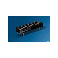
... High Efficiency Red Green High Efficiency Green SCD55104A Slimline DESCRIPTION The SCD55100A (Red), SCD55101A (Yellow), SCD55102A (HER), SCD55103A (Green) and SCD55104A (HEG) are eight digit dot addressable matrix, Serial Input, Intelligent Display devices. The ten 3.68 mm (0.145") high digits are packaged in a rugged, high quality optically transparent, standard 7.62 mm (0.3" ...
Page 2
... SCD55100A, SCD55101A, SCD55102A, SCD55103A, SCD55104A Ordering Information Type Color of Emission SCD55104A standard red SCD55101A yellow SCD55102A high efficiency red SCD55103A green SCD55104A high efficiency green Package Outlines Color Code Part No SCD5510XA OSRAM YYWW 33.02 (1.300) ref. 38.1 (1.500) max. 2.03 (0.080) ...
Page 3
... SCD55100A, SCD55101A, SCD55102A, SCD55103A, SCD55104A Maximum Ratings Parameter Operating temperature range Storage temperature range DC Supply Voltage Input Voltage Levels Relative to GND Solder Temperature 1.59 mm (0.063“) below seating plane, t < 5.0 s Relative Humidity ESD (100 pF, 1.5 kΩ) Input Current Power Dissipation at 85°C ...
Page 4
... SCD55100A, SCD55101A, SCD55102A, SCD55103A, SCD55104A Data Write Cycle LOAD DATA SDCLK T SDCW Instruction Cycle LOAD SDCLK D0 DATA LOAD SDCLK DATA D0 Maximum Power Dissipation vs. Temperature 2008-07-22 T LDS SDCW T Period SDCLK 4 3.5 3.0 2.5 2.0 θ ˚C/W JA 1.5 1.0 0.5 0 -40 - LDH T BL ...
Page 5
... SCD55100A, SCD55101A, SCD55102A, SCD55103A, SCD55104A Electrical Characteristics (over operating temperature) Parameter V CC (4) (Pwr Dwn Mode digits 16 dots/character CC Input current Input current (CLK I/O) OH (CLK I/ θ External Clock Input Frequency 120 ext F Internal Clock Input Frequency 120 osc Clock I/O Bus Loading ...
Page 6
... SCD55100A, SCD55101A, SCD55102A, SCD55103A, SCD55104A Pin Assignment Pin Function Pin 1 SDCLK 28 2 LOAD RST 16 14 GND 15 Switching Specifications (over operating temperature range and V Symbol Description T Reset Active Time RC Load Setup Time T LDS Data Setup Time Clock Period SDCLK Clock Width T SDCW ...
Page 7
... SCD55100A, SCD55101A, SCD55102A, SCD55103A, SCD55104A Display Column and Row Format Row Row Row Row Row Column Data Ranges Row 0 00H to 1FH Row 1 20H to 3FH Row 2 40H to 5FH Row 3 60H to 7FH Row 4 80H to 9FH SCD5510XA Block Diagram MUX CLK I/O MUX Clock SEL ...
Page 8
... SCD55100A, SCD55101A, SCD55102A, SCD55103A, SCD55104A The following explains how to format the serial data to be loaded into the display. The user supplies a string of bit mapped decoded characters. The contents of this string is shown in Figure „Loading Serial Character Data a“ (page 8). Figure „Loading Serial Charac- ter Data b“ ...
Page 9
... SCD55100A, SCD55101A, SCD55102A, SCD55103A, SCD55104A Load Character Address Op code Character Address Load Column Data Op code Column Data The user can activate four Control functions. These include: LED Brightness Level, Lamp Test, IC Power Down, or Display Clear. OPCODEs and five bit words are used to initiate these functions. ...
Page 10
... Soldering Considerations The SCD55100A/1A/2A/3A/4A can be hand soldered with SN63 solder using a grounded iron set to 260°C. Wave soldering is also possible following these conditions: Pre- heat that does not exceed 93°C on the solder side of the PC board or a package surface temperature of 85° ...
Page 11
... SCD55100A, SCD55101A, SCD55102A, SCD55103A, SCD55104A For further information refer to Appnotes 18 and 19 at www.osram-os.com An alternative to soldering and cleaning the display modules is to use sockets. Naturally, 28 pin DIP sockets 7.62 mm (0.300") wide with 2.54 mm (0.100") centers work well for single displays. Multiple display assemblies are best handled by longer SIP sockets or DIP sockets when available for uniform package alignment. Socket manufacturers are Aries Electronics, Inc., Frenchtown, NJ ...
Page 12
... SCD55100A, SCD55101A, SCD55102A, SCD55103A, SCD55104A Additional contrast enhancement is gained by shading the displays. Plastic band-pass filters with built-in louvers offer the next step up in contrast improvement. Plastic filters can be improved further with anti-reflective coatings to reduce glare. The trade-off is fuzzy characters. Mounting the filters close to the display reduces this effect. Take care not to overheat the plastic filter by allowing for proper air flow. ...
Page 13
... SCD55100A, SCD55101A, SCD55102A, SCD55103A, SCD55104A SCD5510XA Interface with Motorola 68HC05C4 Microprocessor (using SPI port OSC1 39 OSC2 SCLK MOSI 68HC05C4 1 RST 9 PA2 20 Cascading Multiple Displays Multiple displays can be cascaded using the CLKSEL and CLK I/O pins as shown below. The display designated as the Master Clock source should have its CLKSEL pin tied high and the slaves should have their CLKSEL pins tied low ...
Page 14
... SCD55100A, SCD55101A, SCD55102A, SCD55103A, SCD55104A Loading Data Into the Display Use following procedure to load data into the display: 1. Power up the display. 2. Bring RST low (600 ns duration minimum) to clear the Multi- plex Counter, Address Register, Control Word Register, User Ram and Data Register. The display will be blank. Dis- play brightness is set to 100%. Data Contents for the Word “ ...
Page 15
... SCD55100A, SCD55101A, SCD55102A, SCD55103A, SCD55104A User Definable Character Set Examples* Upper and Lower Case Alphabets HEX HEX CODE CODE Numerals and Punctuation HEX HEX CODE CODE *CAUTION: No more than 128 LEDs “on” at one time at 100% brightness. 2008-07-22 HEX HEX HEX ...
Page 16
... SCD55100A, SCD55101A, SCD55102A, SCD55103A, SCD55104A User Definable Character Set Examples* (continued) Scientific Notations, etc. HEX HEX CODE CODE Foreign Characters HEX HEX CODE CODE *CAUTION: No more than 128 LEDs “on” at one time at 100% brightness. 2008-07-22 HEX HEX HEX HEX CODE ...
Page 17
... SCD55100A, SCD55101A, SCD55102A, SCD55103A, SCD55104A Revision History: 2008-07-22 Previous Version: 2006-02-20 Page Subjects (major changes since last revision) all Lead free device 6 Pin assignment corrected ublished by P OSRAM Opto Semiconductors GmbH Wernerwerkstrasse 2, D-93049 Regensburg www.osram-os.com © All Rights Reserved. Attention please! The information describes the type of component and shall not be considered as assured characteristics ...