IPD2133 OSRAM Opto Semiconductors Inc, IPD2133 Datasheet - Page 7
IPD2133
Manufacturer Part Number
IPD2133
Description
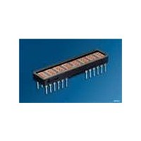
DISPLAY 8DIGIT CERAMIC GREEN
Manufacturer
OSRAM Opto Semiconductors Inc
Series
Alphanumeric Programmable Display™r
Datasheet
1.IPD2131.pdf
(16 pages)
Specifications of IPD2133
Millicandela Rating
500µcd
Size / Dimension
1.68" L x 0.39" W x 0.21" H (42.7mm x 4.8mm x 5.3mm)
Color
Green
Configuration
5 x 7
Number Of Digits
8
Character Size
0.2 in
Illumination Color
High Efficiency Green
Wavelength
568 nm
Maximum Operating Temperature
+ 100 C
Minimum Operating Temperature
- 55 C
Luminous Intensity
500 ucd
Viewing Area (w X H)
2.8 mm x 4.8 mm
Display Type
5 x 7 Dot Matrix
Emitting Color
Hi-Eff. Green
Digit Size (in)
.2in
Viewing Area Height (mm)
4.8mm
Viewing Area Length (mm)
2.8mm
Package Type
Panel
Operating Supply Voltage (min)
4.5V
Operating Supply Voltage (typ)
5V
Operating Supply Voltage (max)
5.5V
Operating Temperature Classification
Industrial
Operating Temp Range
-55C to 100C
Mounting
Through Hole
Pin Count
24
Total Thickness (mm)
4.6mm
Opto Display Type
Panel
Pattern Type
Dot Matrix
Lead Free Status / RoHS Status
Lead free / RoHS Compliant
Voltage - Forward (vf) Typ
-
Internal Connection
-
Lead Free Status / Rohs Status
Compliant
Other names
Q68000A8906
Available stocks
Company
Part Number
Manufacturer
Quantity
Price


Pin Description
Pin No.
1
2
3
4
5
6
7
8
9
10
11
12
13
14
15
16
17
18
19
20
21
22
23
24
25
26
27
28
29
30
31
32
2006-04-04
Function
CLS
CLK
WR
CE
RST
RD
No Pin
D0
D1
D2
D3
NC
V
GND
GND
D4
D5
D6
D7
No Pin
FL
A0
A1
A2
A3
A4
CC
Description
Clock Select
Clock I/O
Write
Chip Enable
Reset
Read
—
Data Bus
—
—
Supply
Logic
Data Bus
—
Flash
Address Inputs
Explanation
Selects an internal or external clock source. CLS=1 the internal clock selected
(master clock), CLS=0 then external clock selected (slave operation).
Inputs or outputs the clock as determined by the CLS pin.
Writes data into the display when WR=0 and CE=0.
Enables the read/write access when low.
Initializes the display; clears the Character RAM (20 Hex), Flash RAM
(00 Hex), Control Word (00 Hex) and resets the internal counters. UDC Address
Register and UDC RAM are unaffected.
Outputs data from the display when RD=0 and CE=0.
—
8 bit bidirectional data bus. Character RAM and Control Word uses D7–D0, UDC
Address Register uses D3–D0, UDC RAM uses D4–D0, and Flash RAM uses D0.
—
Positive power supply.
Analog ground for the LED drivers.
Digital ground for the logic circuitry.
8 bit bidirectional data bus. Character RAM and Control Word uses D7-D0, UDC
Address Register uses D3-D0, UDC RAM uses D4-D0, and Flash RAM uses D0.
—
Accesses the Flash RAM. Address inputs, A2–A0, select the digit address while
data bit D0 sets (D0=1) or resets (D0=0) the Flash bit. A4 and A3 are ignored.
A4 and A3 select a section of the display’s memory. A2–A0 select specific locations
in the different sections. If FL is low the Flash RAM is accessed regardless of the
status of A4 and A3.
7
IPD2131, IPD2132, IPD2133
Related parts for IPD2133
Image
Part Number
Description
Manufacturer
Datasheet
Request
R

Part Number:
Description:
INTELLIGENT DISP 4CHAR 5X7 HERED
Manufacturer:
OSRAM Opto Semiconductors Inc
Datasheet:

Part Number:
Description:
EMITTER IR 950NM 5MM SMD RADIAL
Manufacturer:
OSRAM Opto Semiconductors Inc
Datasheet:

Part Number:
Description:
LED TOPLED GREEN 570NM 2-PLCC
Manufacturer:
OSRAM Opto Semiconductors Inc
Datasheet:

Part Number:
Description:
INTERRUPTER RELFECT W/FILTR SMD
Manufacturer:
OSRAM Opto Semiconductors Inc
Datasheet:

Part Number:
Description:
LED Displays 5x7 Green 0.145 , 4-CHARACTER
Manufacturer:
OSRAM Opto Semiconductors Inc
Datasheet:

Part Number:
Description:
Q65110A4321_SIDELED PURE GREEN EOL150407
Manufacturer:
OSRAM Opto Semiconductors Inc
Datasheet:
Part Number:
Description:
Q65110A1202_RO DETECTOR 3/5MM_TR_RO
Manufacturer:
OSRAM Opto Semiconductors Inc
Datasheet:

Part Number:
Description:
PHOTODIODE 900NM 3MM W/FILTER
Manufacturer:
OSRAM Opto Semiconductors Inc
Datasheet:

Part Number:
Description:
PHOTODIODE 860NM 3MM CLEAR
Manufacturer:
OSRAM Opto Semiconductors Inc
Datasheet:
Part Number:
Description:
INTELLIGENT DISP 4CHAR 5X7 HERED
Manufacturer:
OSRAM Opto Semiconductors Inc
Datasheet:
Part Number:
Description:
LED TOPLED GREEN 570NM 2-PLCC
Manufacturer:
OSRAM Opto Semiconductors Inc
Datasheet:
Part Number:
Description:
PHOTODIODE 900NM 3MM W/FILTER
Manufacturer:
OSRAM Opto Semiconductors Inc
Datasheet:

Part Number:
Description:
PHOTODIODE 850NM THRU-HOLE
Manufacturer:
OSRAM Opto Semiconductors Inc
Datasheet:

Part Number:
Description:
PHOTODIODE 880NM W/FILTER SMD
Manufacturer:
OSRAM Opto Semiconductors Inc
Datasheet: