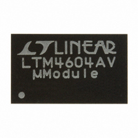
LTM4604AEV#PBF Linear Technology, LTM4604AEV#PBF Datasheet - Page 3

LTM4604AEV#PBF
Manufacturer Part Number
LTM4604AEV#PBF
Description
IC UMODULE DC/DC LV 4A 66-LGA
Manufacturer
Linear Technology
Series
µModuler
Type
Point of Load (POL) Non-Isolatedr
Datasheet
1.LTM4604AEVPBF.pdf
(20 pages)
Specifications of LTM4604AEV#PBF
Design Resources
LTM4604A Spice Model
Output
0.8 ~ 5 V
Number Of Outputs
1
Power (watts)
20W
Mounting Type
Surface Mount
Voltage - Input
2.38 ~ 5.5 V
Package / Case
66-LGA
1st Output
0.8 ~ 5 VDC @ 4A
Size / Dimension
0.59" L x 0.35" W x 0.09" H (15mm x 9mm x 2.3mm)
Power (watts) - Rated
20W
Operating Temperature
-40°C ~ 125°C
Efficiency
95%
Lead Free Status / RoHS Status
Lead free / RoHS Compliant
3rd Output
-
2nd Output
-
Available stocks
Company
Part Number
Manufacturer
Quantity
Price
ELECTRICAL CHARACTERISTICS
Note 1: Stresses beyond those listed under Absolute Maximum Ratings
may cause permanent damage to the device. Exposure to any Absolute
Maximum Rating condition for extended periods may affect device
reliability and lifetime.
Note 2: The LTM4604AE is guaranteed to meet performance specifi cations
over the 0°C to 125°C internal operating temperature range. Specifi cations
over the full –40°C to 125°C internal operating temperature range are assured
operating temperature range, otherwise specifi cations are at T
SYMBOL
I
Output Specifi cations
I
ΔV
ΔV
V
f
ΔV
t
ΔV
t
I
Control Section
V
I
V
I
V
V
R
PGOOD
ΔV
R
S(VIN)
OUT(DC)
S
START
SETTLE
OUT(PK)
FB
TRACK
OUT(AC)
FB
RUN
TRACK(OFFSET)
TRACK(RANGE)
FBHI
PGOOD
OUT(LINE)
OUT(LOAD)
OUT(START)
OUT(LS)
PGOOD
V
V
OUT
OUT
PARAMETER
Input Supply Current
Output Continuous Current
Range (Note 3)
Line Regulation Accuracy
Load Regulation Accuracy
Output Ripple Voltage
Output Ripple Voltage
Frequency
Turn-On Overshoot
Turn-on Time
Peak Deviation for Dynamic
Load Step
Settling Time for Dynamic
Load Step
Output Current Limit
Voltage at FB Pin
RUN Pin On/Off Threshold
TRACK Pin Current
Offset Voltage
Tracking Input Range
Resistor Between V
FB Pins
PGOOD Range
PGOOD Resistance
OUT
and
CONDITIONS
V
V
V
V
V
V
I
I
V
I
V
and RUN/SS = Float
Load: 0% to 50% to 0% of Full Load,
C
Load: 0% to 50% to 0% of Full Load
I
TRACK = 0.4V
Open-Drain Pull-Down
OUT
OUT
OUT
OUT
V
V
V
V
V
V
V
V
V
V
V
V
IN
IN
IN
IN
OUT
OUT
OUT
OUT
OUT
IN
IN
IN
IN
IN
IN
IN
IN
IN
IN
IN
IN
= 2.5V, V
= 3.3V, V
= 5V, V
= 3.3V, V
= 0A
= 4A, V
= 0A
= 0A, V
= 3.3V
= 5V
= 3.3V, V
= 5V, V
= 3.3V
= 5V
= 3.3V
= 5V
= 5V, V
= 5V, V
= 3.3V, V
= 5V, V
= 1.5V, V
= 1.5V, 0A to 4A (Note 3)
= 1.5V, RUN/SS = 10nF,
= 1.5V, I
= 22μF ×3 Ceramic
OUT
OUT
IN
OUT
OUT
OUT
OUT
OUT
OUT
OUT
The
OUT
OUT
OUT
IN
= 5V, V
= 1.5V, I
= 1.5V
= 1.5V
= 1.5V
= 1.5V
= 1.5V
from 2.375V to 5.5V, I
= 1.5V, I
= 1.5V, I
= 1.5V
A
= 1A Resistive Load, TRACK = V
●
= 1.5V
= 1.5V
= 25°C. V
denotes the specifi cations which apply over the full internal
OUT
OUT
OUT
OUT
by design, characterization and correlation with statistical process controls.
The LTM4604AI is guaranteed to meet specifi cations over the full internal
operating temperature range. Note that the maximum ambient temperature
is determined by specifi c operating conditions in conjunction with board
layout, the rated package thermal resistance and other environmental factors.
Note 3: See output current derating curves for different V
= 1.5V
= 4A
= 4A
= 4A
IN
= 5V unless otherwise noted. See Figure 15.
OUT
= 0A
IN
●
●
●
●
0.793
0.788
4.975
MIN
0.5
0
LTM4604A
1.45
1.25
0.65
4.99
TYP
±7.5
2.2
0.2
0.2
2.9
0.1
0.3
0.3
1.5
1.0
0.8
0.8
20
20
25
30
90
10
12
10
8
8
IN
, V
0.807
0.808
5.025
MAX
150
0.2
0.6
0.6
0.8
0.8
4
OUT
and T
UNITS
mV
mV
4604af
3
MHz
A
mV
mV
mV
mV
kΩ
P-P
P-P
ms
ms
μA
μA
.
μs
%
%
%
%
Ω
A
A
A
A
A
A
V
V
V
V


