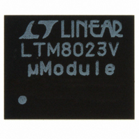
LTM8023IV#PBF Linear Technology, LTM8023IV#PBF Datasheet - Page 13

LTM8023IV#PBF
Manufacturer Part Number
LTM8023IV#PBF
Description
IC BUCK SYNC ADJ 2A 50LGA
Manufacturer
Linear Technology
Series
µModuler
Type
Point of Load (POL) Non-Isolatedr
Datasheet
1.LTM8023EVPBF.pdf
(20 pages)
Specifications of LTM8023IV#PBF
Design Resources
LTM8023 Spice Model
Output
0.8 ~ 10 V
Number Of Outputs
1
Power (watts)
20W
Mounting Type
Surface Mount
Voltage - Input
3.6 ~ 36 V
Package / Case
50-LGA
1st Output
0.8 ~ 10 VDC @ 2A
Size / Dimension
0.44" L x 0.35" W x 0.11" H (11.25mm x 9mm x 2.82mm)
Power (watts) - Rated
20W
Operating Temperature
-40°C ~ 85°C
Lead Free Status / RoHS Status
Lead free / RoHS Compliant
3rd Output
-
2nd Output
-
Available stocks
Company
Part Number
Manufacturer
Quantity
Price
APPLICATIONS INFORMATION
4. Place the C
5. Connect all of the GND connections to as large a copper
6. Use vias to connect the GND copper area to the boards
Hot-Plugging Safely
The small size, robustness and low impedance of ceramic
capacitors make them an attractive option for the input
bypass capacitor of LTM8023. However, these capacitors
can cause problems if the LTM8023 is plugged into a live
supply (see Linear Technology Application Note 88 for
a complete discussion). The low loss ceramic capacitor
combined with stray inductance in series with the power
source forms an underdamped tank circuit, and the voltage
at the V
input voltage, possibly exceeding the LTM8023’s rating and
damaging the part. If the input supply is poorly controlled
or the user will be plugging the LTM8023 into an energized
supply, the input network should be designed to prevent
this overshoot. Figure 6 shows the waveforms that result
when an LTM8023 circuit is connected to a 24V supply
through six feet of 24-gauge twisted pair. The fi rst plot is
the response with a 2.2μF ceramic capacitor at the input.
The input voltage rings as high as 35V and the input current
peaks at 20A. One method of damping the tank circuit is to
add another capacitor with a series resistor to the circuit.
In Figure 6b an aluminum electrolytic capacitor has been
added. This capacitor’s high equivalent series resistance
damps the circuit and eliminates the voltage overshoot. The
extra capacitor improves low frequency ripple fi ltering and
can slightly improve the effi ciency of the circuit, though
it is likely to be the largest component in the circuit. An
alternative solution is shown in Figure 6c. A 0.7Ω resistor
is added in series with the input to eliminate the voltage
overshoot (it also reduces the peak input current). A 0.1μF
ground current fl ow directly adjacent or underneath
the LTM8023.
pour or plane area as possible on the top layer. Avoid
breaking the ground connection between the external
components and the LTM8023.
internal ground plane. Liberally distribute these GND
vias to provide both a good ground connection and
thermal path to the internal planes of the printed circuit
board.
IN
pin of the LTM8023 can ring to twice the nominal
IN
and C
OUT
capacitors such that their
capacitor improves high frequency fi ltering. This solution is
smaller and less expensive than the electrolytic capacitor.
For high input voltages its impact on effi ciency is minor,
reducing effi ciency less than one-half percent for a 5V
output at full load operating from 24V.
Thermal Considerations
The LTM8023 output current may need to be derated if it
is required to operate in a high ambient temperature or
deliver a large amount of continuous power. The amount of
current derating is dependent upon the input voltage, output
power and ambient temperature. The derating curves
given in the Typical Performance Characteristics section
can be used as a guide. These curves were generated by a
LTM8023 mounted to a 33cm
board. Boards of other sizes and layer count can exhibit
different thermal behavior, so it is incumbent upon the user
to verify proper operation over the intended system’s line,
load and environmental operating conditions.
The junction to air and junction to board thermal resistances
given in the Pin Confi guration diagram may also be used
to estimate the LTM8023 internal temperature. These
thermal coeffi cients are determined per JESD 51-9 (JEDEC
standard, test boards for area array surface mount package
thermal measurements) through analysis and physical
correlation. Bear in mind that the actual thermal resistance
of the LTM8023 to the printed circuit board depends upon
the design of the circuit board. The die temperature of
the LTM8023 must be lower than the maximum rating of
125°C, so care should be taken in the layout of the circuit
to ensure good heat sinking of the LTM8023.
The bulk of the heat fl ow out of the LTM8023 is through the
bottom of the module and the LGA pads into the printed
circuit board. Consequently a poor printed circuit board
design can cause excessive heating, resulting in impaired
performance or reliability. Please refer to the PCB Layout
section for printed circuit board design suggestions.
Finally, be aware that at high ambient temperatures the
internal Schottky diode will have signifi cant leakage current
(see Typical Performance Characteristics) increasing the
quiescent current of the LTM8023.
2
4-layer FR4 printed circuit
LTM8023
13
8023ff


