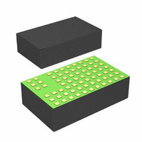
LTM8031IV#PBF Linear Technology, LTM8031IV#PBF Datasheet - Page 7

LTM8031IV#PBF
Manufacturer Part Number
LTM8031IV#PBF
Description
IC BUCK ADJ 1A 71LGA
Manufacturer
Linear Technology
Series
µModuler
Type
Point of Load (POL) Non-Isolatedr
Datasheet
1.LTM8031EVPBF.pdf
(20 pages)
Specifications of LTM8031IV#PBF
Design Resources
LTM8031 Spice Model
Output
0.8 ~ 10 V
Number Of Outputs
1
Power (watts)
10W
Mounting Type
Surface Mount
Voltage - Input
3.6 ~ 36 V
Package / Case
71-LGA
1st Output
0.8 ~ 10 VDC @ 1A
Size / Dimension
0.59" L x 0.35" W x 0.11" H (15mm x 9mm x 2.8mm)
Power (watts) - Rated
10W
Operating Temperature
-40°C ~ 125°C
Approvals
EN
Lead Free Status / RoHS Status
Lead free / RoHS Compliant
3rd Output
-
2nd Output
-
PIN FUNCTIONS
SYNC (Pin L6): This is the external clock synchronization
input. Ground this pin for low ripple Burst Mode
at low output loads. Tie to a stable voltage source greater
than 0.7V to disable Burst Mode operation. Do not leave
this pin fl oating. Tie to a clock source for synchroniza-
tion. Clock edges should have rise and fall times faster
than 1μs. See Synchronization section in Applications
Information.
PGOOD (Pin K7): The PGOOD pin is the open-collector
output of an internal comparator. PGOOD remains low until
the ADJ pin is within 10% of the fi nal regulation voltage.
BLOCK DIAGRAM
FIN
V
GND
SHARE
IN
EMI FILTER
RUN/SS
SYNC
CONTROLLER
CURRENT
®
MODE
operation
RT
The PGOOD output is valid when V
RUN/SS is high. If this function is not used, leave this
pin fl oating.
ADJ (Pin J7): The LTM8031 regulates its ADJ pin to 0.79V.
Connect the adjust resistor from this pin to ground. The
value of R
where R
Burst Mode is a registered trademark of Linear Technology Corporation.
PGOOD
R
ADJ
ADJ
=
ADJ
V
OUT
is in kΩ.
196 71
is given by the equation:
4.7μH
– .
.
0 79
22pF
ADJ
249k
10μF
IN
V
BIAS
GND
AUX
is above 3.6V and
OUT
LTM8031
8031 BD
8031fa
7


