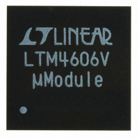
LTM4606EV#PBF Linear Technology, LTM4606EV#PBF Datasheet - Page 20

LTM4606EV#PBF
Manufacturer Part Number
LTM4606EV#PBF
Description
IC DC/DC UMODULE 6A 133-LGA
Manufacturer
Linear Technology
Series
µModuler
Type
Point of Load (POL) Non-Isolatedr
Datasheet
1.LTM4606EVPBF.pdf
(28 pages)
Specifications of LTM4606EV#PBF
Design Resources
LTM4606 Spice Model
Output
0.6 ~ 5 V
Number Of Outputs
1
Power (watts)
30W
Mounting Type
Surface Mount
Voltage - Input
4.5 ~ 28 V
Package / Case
133-LGA
1st Output
0.6 ~ 5 VDC @ 6A
Size / Dimension
0.59" L x 0.59" W x 0.11" H (15mm x 15mm x 2.8mm)
Power (watts) - Rated
30W
Operating Temperature
-40°C ~ 125°C
Efficiency
93%
Lead Free Status / RoHS Status
Lead free / RoHS Compliant
3rd Output
-
2nd Output
-
Available stocks
Company
Part Number
Manufacturer
Quantity
Price
applicaTions inForMaTion
LTM4606
Frequency Adjustment
The LTM4606 is designed to typically operate at 800kHz
across most input conditions. The f
open or decoupled with an optional 1000pF capacitor. The
switching frequency has been optimized for maintaining
constant output ripple noise over most operating ranges.
The 800kHz switching frequency and the 400ns minimum
off time can limit operation at higher duty cycles like 5V
to 3.3V, and produce excessive inductor ripple currents
for lower duty cycle applications like 28V to 5V.
Example for 5V Output
Equations for setting frequency:
I
For 28V input operation, I
I
(28 • 211ns)) ~ 850kHz. The inductor ripple current begins
to get high at the higher input voltages due to a larger volt-
age across the inductor. The current ripple is ~5A at 20%
duty cycle if the integrated inductor is 1µH. The inductor
ripple current can be lowered at the higher input voltages by
adding an external resistor from f
the switching frequency. A 4A ripple current is chosen, and
the total peak current is equal to 1/2 of the 4A ripple current
plus the output current. For 5V output, current is limited to
5A, so the total peak current is less than 7A. This is below
the 8A peak specified value. A 150k resistor is placed from
f
41.2k equates to 32.3k. The I
and 28V input voltage equals 289µA. This equates to a t
of 166ns. This will increase the switching frequency from
850kHz to ~1MHz for the 28V to 5V conversion. The
minimum on time is above 100ns at 28V input. Since
the switching frequency is approximately constant over
input and output conditions, then the lower input voltage
range is limited to 8V for the 1MHz operation due to the
400ns minimum off time. Equation: t
Frequency) equates to a 375ns on time, and a 400ns off
20
fSET
fSET
SET
LTM4606 minimum on-time = 100ns;
t
LTM4606 minimum off-time = 400ns;
t
Duty Cycle = t
ON
OFF
), t
to ground, and the parallel combination of 150k and
= (V
= ((4.8 • 10pF)/I
= t – t
ON
IN
= 211ns. Frequency = (V
/(3 • R
ON
, where t = 1/Frequency
ON
fSET
/t or V
)), where the internal R
fSET
fSET
OUT
)
/V
= 227µA. t
fSET
IN
SET
calculation with 32.3k
OUT
SET
to ground to increase
ON
/(V
pin is typically left
ON
= (V
IN
= ((4.8 • 10pF)/
• t
OUT
fSET
ON
/V
is 41.2k.
)) = (5V/
IN
) • (1/
ON
time. Figure 18 shows an operating range of 10V to 28V for
1MHz operation with a 150k resistor to ground, and an 8V to
16V operating range for f
are made to provide wider input voltage ranges for the 5V
output designs while limiting the inductor ripple current,
and maintaining the 400ns minimum off-time.
Example for 3.3V Output
Equations for setting frequency:
I
227µA, t
internal R
(3.3V/(28 • 145ns)) ~ 810kHz. The minimum on-time and
minimum-off time are within specification at 146ns and
1089ns. But the 4.5V minimum input for converting 3.3V
output will not meet the minimum off-time specification
of 400ns. t
Solution
Lower the switching frequency at lower input voltages to
allow for higher duty cycles, and meet the 400ns mini-
mum off-time at 4.5V input voltage. The off-time should
be about 500ns with 100ns guard band. The duty cycle
for (3.3V/4.5V) = ~73%. Frequency = (1 – DC)/t
(1 – 0.73)/500ns = 540kHz. The switching frequency
needs to be lowered to 540kHz at 4.5V input. t
frequency, or 1.35µs. The f
is 1/3 of V
the internal 41.2k. The I
540kHz operation. A resistor can be placed from V
f
to 24µA. The f
therefore a 150k resistor will source 12µA into the f
node and lower the I
540kHz operation and the 4.5V to 28V input operation for
down converting to 3.3V output as shown in Figure 19.
The frequency will scale from 540kHz to 950kHz over this
input range. This provides for an effective output current
of 5A over the input range.
fSET
SET
LTM4606 minimum on-time = 100ns;
t
LTM4606 minimum off-time = 400ns;
t
Duty Cycle (DC) = t
ON
OFF
to lower the effective I
= (V
= ((3.3 • 10pF)/I
= t – t
ON
IN
fSET
ON
IN
/(3 • R
= ((3.3 • 10pF)/I
, and the I
ON
= 905ns, Frequency = 810kHz, t
is 41.2k. Frequency = (V
SET
, where t = 1/Frequency
fSET
pin is 4.5V/3 =1.5V and V
fSET
)), for 28V input operation, I
ON
fSET
fSET
fSET
current to 24µA. This enables the
SET
/t or V
)
fSET
current equates to 36µA with
fSET
floating. These modifications
current needs to be 24µA for
SET
OUT
current out of the f
), t
pin voltage compliance
/V
ON
IN
= 145ns, where the
OUT
/(V
OFF
OUT
IN
ON
= 329ns.
• t
SET
= 3.3V,
ON
OFF
OUT
fSET
= DC/
4606fb
)) =
SET
pin
or
to
=


