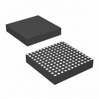
LTM4619EV#PBF Linear Technology, LTM4619EV#PBF Datasheet - Page 17

LTM4619EV#PBF
Manufacturer Part Number
LTM4619EV#PBF
Description
IC SWIT REG BUCK 4A ADJ 144LGA
Manufacturer
Linear Technology
Series
µModuler
Type
Point of Load (POL) Non-Isolatedr
Datasheet
1.LTM4619EVPBF.pdf
(24 pages)
Specifications of LTM4619EV#PBF
Design Resources
LTM4619 Spice Model
Output
0.8 ~ 5 V
Number Of Outputs
2
Power (watts)
30W
Mounting Type
Surface Mount
Voltage - Input
4.5 ~ 26.5 V
Package / Case
144-LGA
1st Output
0.8 ~ 5 VDC @ 4A
2nd Output
0.8 ~ 5 VDC @ 4A
Size / Dimension
0.59" L x 0.59" W x 0.11" H (15mm x 15mm x 2.8mm)
Power (watts) - Rated
30W
Operating Temperature
-40°C ~ 125°C
Lead Free Status / RoHS Status
Lead free / RoHS Compliant
3rd Output
-
Available stocks
Company
Part Number
Manufacturer
Quantity
Price
applicaTions inForMaTion
Layout Checklist/Example
The high integration of LTM4619 makes the PCB board
layout very simple and easy. However, to optimize its electri-
cal and thermal performance, some layout considerations
are still necessary.
• Use large PCB copper areas for high current path, includ-
• Place high frequency ceramic input and output capaci-
• Place a dedicated power ground layer underneath the
ing V
the PCB conduction loss and thermal stress.
tors next to the V
high frequency noise.
unit.
IN
, PGND, V
OUT1
IN
, PGND and V
PGND
and V
OUT2
V
OUT2
C
IN2
. It helps to minimize
OUT
M
K
H
G
D
C
B
A
L
J
F
E
C
1
OUT2
pins to minimize
Figure 17. Recommended PCB Layout
2
3
4
5
TOP VIEW
6
PGND
V
IN
7
• To minimize the via conduction loss and reduce module
• Do not put vias directly on the pad.
• Use a separated SGND ground copper area for com-
• Decouple the input and output grounds to lower the
Figure 17 gives a good example of the recommended layout.
thermal stress, use multiple vias for interconnections
between top layer and other power layers.
ponents connected to signal pins. Connect the SGND
to PGND underneath the unit.
output ripple noise. Refer to Figure 17.
8
9
10
11
C
OUT1
12
C
IN1
V
OUT1
PGND
LTM4619
17
4619fa


