LTM4612IV#PBF Linear Technology, LTM4612IV#PBF Datasheet - Page 3
LTM4612IV#PBF
Manufacturer Part Number
LTM4612IV#PBF
Description
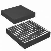
IC BUCK SYNC ADJ 5A 133LGA
Manufacturer
Linear Technology
Series
µModuler
Type
Point of Load (POL) Non-Isolatedr
Datasheet
1.LTM4612EVPBF.pdf
(26 pages)
Specifications of LTM4612IV#PBF
Design Resources
LTM4612 Spice Model
Output
3.3 ~ 15 V
Number Of Outputs
1
Power (watts)
75W
Mounting Type
Surface Mount
Voltage - Input
5 ~ 36 V
Package / Case
133-LGA
1st Output
3.3 ~ 15 VDC @ 5A
Size / Dimension
0.59" L x 0.59" W x 0.11" H (15mm x 15mm x 2.8mm)
Power (watts) - Rated
75W
Operating Temperature
-40°C ~ 125°C
Dc To Dc Converter Type
Non-Inverting/Inverting/Step Up/Step Down
Pin Count
133
Input Voltage
36V
Output Voltage
3.3 to 15V
Switching Freq
940KHz
Output Current
5A
Package Type
LGA
Output Type
Adjustable
Switching Regulator
Yes
Load Regulation
0.6%
Line Regulation
0.3%
Mounting
Surface Mount
Input Voltage (min)
5V
Operating Temperature Classification
Automotive
Lead Free Status / RoHS Status
Lead free / RoHS Compliant
3rd Output
-
2nd Output
-
Lead Free Status / Rohs Status
Compliant
Available stocks
Company
Part Number
Manufacturer
Quantity
Price


elecTrical characTerisTics
operating temperature range, otherwise specifications are at T
(front page) configuration.
SYMBOL
I
I
V
Output Specifications
I
DV
DV
V
V
f
DV
t
DV
t
I
Control Section
V
V
I
V
I
t
t
R
Q(VIN)
S(VIN)
OUT(DC)
S
START
SETTLE
OUT(PK)
SS / TRACK
FCB
ON(MIN)
OFF(MIN)
INTVCC
IN(AC)
OUT(AC)
FB
RUN
FCB
PLLIN
V
OUT(LINE)
OUT(LOAD)
OUT(START)
OUT(LS)
V
OUT
OUT
PARAMETER
Input Supply Bias Current
Input Supply Current
Internal V
Output Continuous Current Range
Line Regulation Accuracy
Load Regulation Accuracy
Input Ripple Voltage
Output Ripple Voltage
Output Ripple Voltage Frequency
Turn-On Overshoot,
TRACK/SS = 10nF
Turn-On Time, TRACK/SS = Open
Peak Deviation for Dynamic Load
Settling Time for Dynamic Load Step Load: 0% to 50% to 0% of Full Load, V
Output Current Limit
Voltage at V
RUN Pin On/Off Threshold
Soft-Start Charging Current
Forced Continuous Threshold
Forced Continuous Pin Current
Minimum On-Time
Minimum Off-Time
PLLIN Input Resistor
CC
FB
Voltage
Pin
CONDITIONS
V
V
Shutdown, RUN = 0, V
V
V
V
V
V
I
V
I
C
Electrolytic, 1 × 10µF X5R Ceramic on V
I
C
I
C
C
Resistive Load
Load: 0% to 50% to 0% of Full Load
C
C
I
V
V
(Note 3)
(Note 3)
OUT
OUT
OUT
OUT
OUT
IN
IN
IN
IN
IN
IN
OUT
OUT
IN
OUT
OUT
OUT
OUT
OUT
SS/TRACK
FCB
V
V
V
V
V
V
V
V
V
V
V
V
V
= 36V, V
= 24V, V
= 36V, V
= 24V, V
= 24V, V
= 2 × 10µF X5R Ceramic and 1 × 100µF
= 36V, RUN > 2V, I
IN
IN
IN
IN
IN
IN
IN
IN
IN
IN
IN
IN
IN
= 0A
= 0A,
= 0A,
= 1A, V
= 0A, V
= 0V
= 12V, FCB = 0V, V
= 12V, FCB = 0V, I
= 2 × 22µF , 2 × 47µF X5R Ceramic
= 200µF , V
= 300µF , V
= 2 × 22µF Ceramic, 150µF Bulk
= 200µF
The
= 36V
= 24V
= 24V, V
= 24V, V
= 24V, V
= 24V, V
= 36V
= 24V
= 36V
= 24V
= 24V, V
= 36V, V
= 24V, V
= 0V
A
OUT
OUT
OUT
OUT
OUT
l
IN
OUT
= 25°C, V
denotes the specifications which apply over the full internal
= 24V, V
OUT
OUT
OUT
OUT
OUT
OUT
OUT
OUT
OUT
= 12V, Switching Continuous
= 12V, Switching Continuous
= 12V, I
= 12V, I
= 12V (Note 4)
= 12V
= 5V
= 12V
= 5V
= 12V
= 12V
= 12V
= 12V
= 12V, I
= 12V, I
OUT
OUT
IN
OUT
OUT
OUT
IN
IN
= 36V
= 0A
= 22V to 36V,
= 12V
= 24V, unless otherwise noted. Per Typical Application
= 0A to 5A (Note 4)
OUT
OUT
= 5A
= 5A
= 0A
= 1A
IN
D
= 24V
Pins
l
l
l
l
0.591
MIN
0.57
4.7
–1
0
1
1.85
2.72
0.05
17.5
12.5
–1.5
TYP
940
153
250
0.3
0.3
7.2
3.4
0.5
0.5
0.6
1.5
0.6
57
48
50
20
20
37
–1
50
50
5
9
9
LTM4612
0.609
MAX
0.63
100
400
5.3
0.3
0.6
0.6
1.9
–2
–2
5
UNITS
mV
mV
mV
mV
4612fa
kHz
mA
mA
mV
mV
mV
ms
ms
P-P
P-P
P-P
P-P
kW
µA
µA
µA
µs
ns
ns
%
%
%
A
A
V
A
A
A
V
V
V
Related parts for LTM4612IV#PBF
Image
Part Number
Description
Manufacturer
Datasheet
Request
R

Part Number:
Description:
Ultralow Noise 36vin, 15vout, 5a, Dc/dc ?module
Manufacturer:
Linear Technology Corporation
Datasheet:

Part Number:
Description:
BOARD EVAL LTM4612
Manufacturer:
Linear Technology
Datasheet:

Part Number:
Description:
IC BUCK SYNC ADJ 5A 133LGA
Manufacturer:
Linear Technology
Datasheet:
Part Number:
Description:
IC BUCK SYNC ADJ 5A 133LGA
Manufacturer:
Linear Technology
Datasheet:
Part Number:
Description:
CD ROM LINEARVIEW DATASHEETS
Manufacturer:
Linear Technology
Part Number:
Description:
Standalone Linear Li-Ion Battery Charger with Thermal Regulation in ThinSOT
Manufacturer:
Linear Technology Corporation
Datasheet:
Part Number:
Description:
Low noise, high frequency, 8th order linear phase lowpass filter
Manufacturer:
Linear Technology Corporation
Datasheet:
Part Number:
Description:
Manufacturer:
Linear Technology Corporation
Datasheet:
Part Number:
Description:
Manufacturer:
Linear Technology Corporation
Datasheet:
Part Number:
Description:
Manufacturer:
Linear Technology Corporation
Datasheet:
Part Number:
Description:
Manufacturer:
Linear Technology Corporation
Datasheet:
Part Number:
Description:
Manufacturer:
Linear Technology Corporation
Datasheet:
Part Number:
Description:
Manufacturer:
Linear Technology Corporation
Datasheet:
Part Number:
Description:
Manufacturer:
Linear Technology Corporation
Datasheet:
Part Number:
Description:
Dual and Quad, JFET Input Precision High Speed Op Amps
Manufacturer:
Linear Technology Corporation
Datasheet: