LTM4608AMPV#PBF Linear Technology, LTM4608AMPV#PBF Datasheet
LTM4608AMPV#PBF
Specifications of LTM4608AMPV#PBF
Available stocks


Related parts for LTM4608AMPV#PBF


LTM4608AMPV#PBF Summary of contents
Page 1
... Point of Load Regulation n L, LT, LTC, LTM, Linear Technology, the Linear logo, Burst Mode, µModule and PolyPhase are registered trademarks and LTpowerCAD is a trademark of Linear Technology Corporation. All other trademarks are the property of their respective owners. Protected by U.S. Patents including 5481178, 6580258, 6304066, 6127815, 6498466, 6611131. ...
Page 2
... LTM4608AEV#PBF LTM4608AIV#PBF LTM4608AIV#PBF LTM4608AMPV#PBF LTM4608AMPV#PBF LTM4608AMPV Consult LTC Marketing for parts specified with wider operating temperature ranges. *The temperature grade is identified by a label on the shipping container. For more information on lead free part marking, go to: http://www.linear.com/leadfree/ This product is only offered in trays. For more information go to: http://www.linear.com/packaging/ ...
Page 3
ELECTRICAL CHARACTERISTICS operating temperature range, otherwise specifications are at T SYMBOL PARAMETER I Input Supply Bias Current Q(VIN) I Input Supply Current S(VIN) Output Specifications I Output Continuous Current Range OUT(DC) (Note 3) ∆V Line Regulation Accuracy OUT(LINE) V OUT ...
Page 4
LTM4608A ELECTRICAL CHARACTERISTICS operating temperature range, otherwise specifications are at T SYMBOL PARAMETER TRACK Tracking Threshold (Rising) Tracking Threshold (Falling) Tracking Disable Threshold R Resistor Between V and FB FBHI OUT Pins ∆V PGOOD Range PGOOD %Margining Output Voltage Margining ...
Page 5
TYPICAL PERFORMANCE CHARACTERISTICS Efficiency vs Load Current 100 CONTINUOUS MODE 1.2V IN OUT 5V 1.5V IN OUT 5V 1. OUT 5V 2.5V IN OUT 5V 3.3V IN OUT ...
Page 6
LTM4608A TYPICAL PERFORMANCE CHARACTERISTICS Load Transient Response I LOAD 2A/DIV V OUT 20mV/DIV AC COUPLED 4608A G10 20µs/DIV 1.8V 4.87k OUT FB 2.5A/µs STEP C = 100µF X5R OUT C1 = NONE, ...
Page 7
PIN FUNCTIONS V (C1, C8, C9, D1, D3-D5, D7-D9 and E8): Power Input IN Pins. Apply input voltage between these pins and GND pins. Recommend placing input decoupling capacitance directly between V pins and GND pins (C10-C11, D10-D11, ...
Page 8
LTM4608A PIN FUNCTIONS FB (E7): The Negative Input of the Error Amplifier. Internally, this pin is connected to V with a 10k precision resistor. OUT Different output voltages can be programmed with an ad- ditional resistor between FB and GND ...
Page 9
SIMPLIFIED BLOCK DIAGRAM SV IN TRACK MGN BSEL PGOOD MODE RUN CLKIN CLKOUT PHMODE I TH INTERNAL COMP PLLLPF INTERNAL FILTER I THM SGND Table 1. Decoupling Requirements 25°C, Block Diagram Configuration A SYMBOL PARAMETER C External Input ...
Page 10
... As shown in the Block Diagram, a 10k 0.5% internal feedback resistor connects V together. The output voltage will default to 0.596V with 10 conditions. The Linear Technology µModule Power Design Tool is provided for transient and stability analysis. The FB pin is used to program the output voltage with a single external resistor to ground. ...
Page 11
... The table optimizes total equivalent ESR and total bulk capacitance to optimize the transient performance. Stability criteria are considered in the Table 3 matrix, and the Linear Technology LTpowerCAD™ Design Tool is available for stability analysis. Multiphase operation will reduce effective output ripple as a function of the number of phases ...
Page 12
LTM4608A APPLICATIONS INFORMATION Table 3. Output Voltage Response Versus Component Matrix (Refer to Figure 18 Load Step TYPICAL MEASURED VALUES C VENDORS VALUE PART NUMBER OUT1 TDK 22µF , 6.3V C3216X7S0J226M Murata 22µF , 16V GRM31CR61C226KE15L TDK ...
Page 13
APPLICATIONS INFORMATION provide more output current without increasing input and output voltage ripple. The CLKIN pin allows the LTM4608A to synchronize to an external clock (between 0.75MHz and 2.25MHz) and the internal phase locked loop allows the LTM4608A to lock ...
Page 14
LTM4608A APPLICATIONS INFORMATION The LTM4608A device is an inherently current mode con- trolled device. Parallel modules will have very good current sharing. This will balance the thermals on the design. Tie the I pins of each LTM4608A together to share ...
Page 15
APPLICATIONS INFORMATION CLKIN is tied to ground or if it’s driven by an external frequency synchronization signal. A capacitor value of 0.01µF must be placed from the PLLLPF pin to ground to control the slew rate of the spread spectrum ...
Page 16
LTM4608A APPLICATIONS INFORMATION The track pin of the master can be controlled by an external ramp and C in Figure 5 referenced ramp time can be programmed using equation: ...
Page 17
APPLICATIONS INFORMATION Slope Compensation The module has already been internally compensated for all output voltages. Table 3 is provided for most applica- tion requirements. A spice model will be provided for other control loop optimization. For single module operation, connect ...
Page 18
LTM4608A APPLICATIONS INFORMATION 400LFM 1 200LFM 0LFM 100 AMBIENT TEMPERATURE (°C) Figure 9. No Heat Sink with 3. ...
Page 19
APPLICATIONS INFORMATION 400LFM 1 200LFM 0LFM 100 AMBIENT TEMPERATURE (°C) Figure 15. No Heat Sink with 5V Table 4. 1.5V Output DERATING CURVE V (V) ...
Page 20
LTM4608A APPLICATIONS INFORMATION Safety Considerations The LTM4608A modules do not provide isolation from There is no internal fuse. If required, a slow blow OUT fuse with a rating twice the maximum input current needs to be ...
Page 21
TYPICAL APPLICATIONS 5. 10µF MODE PHMODE 5.5V TRACK C2 10µF Figure 19. Two LTM4608As in Parallel, 1.5V at 16A Design. See Also Dual 8A per Channel LTM4616 CLKIN CLKIN V ...
Page 22
LTM4608A TYPICAL APPLICATIONS D1 MMSD4148 SHDN D2 MMSD4148 SHDN Figure 20. Dual LTM4608A Output Sequencing Application. See Also Dual 8A per Channel LTM4616 V IN 2.7V TO 5.5V 0.01µF Figure 21. 2.7V to 5.5V 22 CLKIN CLKIN ...
Page 23
TYPICAL APPLICATIONS LTM4608A 4608afc 23 ...
Page 24
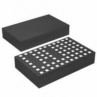
LTM4608A PACKAGE DESCRIPTION PAD “A1” CORNER 4 15.00 BSC X 9.00 Y BSC PACKAGE TOP VIEW 6.350 5.080 3.810 2.540 1.270 0.000 1.270 2.540 3.810 5.080 6.350 SUGGESTED PCB LAYOUT TOP VIEW PACKAGE PHOTO 24 LGA Package 68-Lead (15mm × ...
Page 25
... Added Package Photo Information furnished by Linear Technology Corporation is believed to be accurate and reliable. However, no responsibility is assumed for its use. Linear Technology Corporation makes no representa- tion that the interconnection of its circuits as described herein will not infringe on existing patent rights. conditions in the Electrical Characteristics section. ...
Page 26
... OUT ≤ 5V, 6.25mm × 11.25mm × 2.8mm LGA Package OUT ≤ 10V, 11.25mm × 9mm × 2.8mm LGA Package OUT ≤ 10V, 11.25mm × 9mm × 2.8mm LGA Package OUT LT 0311 REV C • PRINTED IN USA LINEAR TECHNOLOGY CORPORATION 2008 4608afc ...