YV12T25-0G POWER ONE, YV12T25-0G Datasheet
YV12T25-0G
Specifications of YV12T25-0G


Related parts for YV12T25-0G


YV12T25-0G Summary of contents
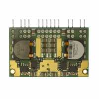
Page 1
... Power-One’s point-of-load converters are recommended for use with regulated bus converters in an Intermediate Bus Architecture (IBA). The YV-Series of non-isolated dc-dc converters deliver Amps of output current in a through-hole (SIP) package. Operating from VDC input, the YV12T25 converter is an ideal choice for Intermediate Bus Architectures where Point-of-Load (POL) power delivery is a requirement. The converter provides an extremely tight regulated programmable output voltage of 0 ...
Page 2
... Note that startup time is the sum of turn-on delay time and rise time. 3 The converter the SEQ/ENA pin is left open. ZD-01983 Rev. 2.1, 25-Jun-10 YV12T25 DC-DC Converter VDC Input; 0.8 - 5.5 VDC Programmable @ 25 A Notes Continuous By external resistor, See Trim Table 1 Full resistive load From Vin = Vin(min ...
Page 3
... Maximum Input Current Input Standby Current (Converter disabled) Input No Load Current (Converter enabled) i Input Reflected-Ripple Current - s Input Voltage Ripple Rejection ZD-01983 Rev. 2.1, 25-Jun-10 YV12T25 DC-DC Converter VDC Input; 0.8 - 5.5 VDC Programmable @ 25 A Notes 25 ADC Output @ 10VDC Input V = 5.0 VDC OUT ...
Page 4
... Settling Time (V < 10% peak deviation) OUT Efficiency General Specifications Parameter Calculated MTBF Weight ZD-01983 Rev. 2.1, 25-Jun-10 YV12T25 DC-DC Converter VDC Input; 0.8 - 5.5 VDC Programmable @ 25 A Notes Full resistive load From no load to full load V = 5.0 VDC OUT All output voltages ...
Page 5
... Internally, the converter has 40 μF (low ESR ceramics) of input capacitance. The YV12T25-0 has been designed for stable operation with or without capacitance ...
Page 6
... ELV. The converter is not internally fused. To comply with safety agencies’ requirements, a recognized fuse with a maximum rating of 30 Amps must be used in series with the input line. www.power-one.com YV12T25 DC-DC Converter Data Sheet [V] R [Ω] TRIM 11 0 ...
Page 7
... The output voltage ripple and input if this reflected ripple current waveforms are obtained using the test setup shown in Fig Source Inductance Vsource Fig. E: Test setup for measuring input reflected-ripple www.power-one.com YV12T25 DC-DC Converter Data Sheet does not exceed a VIN VOUT Cin=150uF Cout = 1uF Ceramic Tantalum Module ...
Page 8
... Vin = 13.2 Vdc Vin = 12.0 Vdc 65 Vin = 10.8 Vdc Fig. 6: Efficiency vs. load current and input voltage for Vout = 1.2 V. www.power-one.com YV12T25 DC-DC Converter Data Sheet Vin = 13.2 Vdc Vin = 12.0 Vdc Vin = 10.8 Vdc Load Current (Adc) Vin = 13.2 Vdc Vin = 12.0 Vdc Vin = 10 ...
Page 9
... Fig. 16: Available load current vs. ambient temperature and airflow rates for Vout = 1.2 V with Vin = 12 V, and maximum MOSFET temperature ≤ 110 °C. Horizontal Orientation (Airflow from Vin pin to GND pin.) www.power-one.com YV12T25 DC-DC Converter Data Sheet 400 LFM 300 LFM 200 LFM ...
Page 10
... Vin = 12 V. Top Trace: Input Voltage Signal (5 V/div.); Bottom Trace: Output Voltage (1 V/div.); Time Scale: 1 ms/div. ZD-01983 Rev. 2.1, 25-Jun-10 YV12T25 DC-DC Converter VDC Input; 0.8 - 5.5 VDC Programmable @ 25 A Fig. 18: Turn-on transient for Vout = 3.3 V and 5.0 V with the application of SEQ/ENA signal at full rated load current (resistive) and 1 μ ...
Page 11
... Vin = 12 V. Top Trace: Output Voltage (100 mV/div.); Bottom Trace: Load Current (10 A/div μF ceramic. Time Scale: 10 μs/div. ZD-01983 Rev. 2.1, 25-Jun-10 YV12T25 DC-DC Converter VDC Input; 0.8 - 5.5 VDC Programmable @ 25 A Fig. 22: Output voltage ripple (20 mV/div.) at full rated load current into a resistive load with external capacitance 1 μ ...
Page 12
... V Through-hole The example above describes P/N YV12T25-0: 10 – input, through-hole (SIP 0 5.5 V output, standard enable logic, and Eutectic Tin/Lead solder. Please consult factory for the complete list of available options. NUCLEAR AND MEDICAL APPLICATIONS - Power-One products are not designed, intended for use in, or authorized for use as critical components in life support systems, equipment used in hazardous environments, or nuclear control systems without the express written consent of the respective divisional president of Power-One, Inc ...