YS12S10-0G POWER ONE, YS12S10-0G Datasheet - Page 8
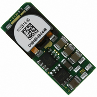
YS12S10-0G
Manufacturer Part Number
YS12S10-0G
Description
CONVERTER DC-DC 12V 10A SMD
Manufacturer
POWER ONE
Series
Yr
Type
Point of Load (POL) Non-Isolatedr
Datasheet
1.YS12S10-0G.pdf
(27 pages)
Specifications of YS12S10-0G
Output
0.75 ~ 5.5V
Number Of Outputs
1
Power (watts)
55W
Mounting Type
Surface Mount
Voltage - Input
9.6 ~ 14V
Package / Case
6-DIP SMD Module
1st Output
0.75 ~ 5.5 VDC @ 10A
Size / Dimension
1.30" L x 0.53" W x 0.31" H (33mm x 13.5mm x 7.9mm)
Power (watts) - Rated
55W
Operating Temperature
-40°C ~ 85°C
Efficiency
95%
Approvals
cUL, EN, UL
Package
6SMD
Output Current
10 A
Output Voltage
0.7525 to 5.5 V
Input Voltage
12 V
Output Power
55 W
Input Voltage Range
9.6 V to 14 V
Input Voltage (nominal)
12 V
Output Voltage (channel 1)
0.7525 V to 5.5 V
Output Current (channel 1)
10 A
Package / Case Size
33.02 mm x 13.46 mm x 7.98 mm
Output Type
Regulated
Product
Non-Isolated / POL
Lead Free Status / RoHS Status
Lead free / RoHS Compliant
3rd Output
-
2nd Output
-
Lead Free Status / Rohs Status
Lead free / RoHS Compliant
Other names
179-2371-2
Available stocks
Company
Part Number
Manufacturer
Quantity
Price
Company:

Part Number:
YS12S10-0G
Manufacturer:
PowerOne
Quantity:
100
Company:
Part Number:
YS12S10-0G
Manufacturer:
STM
Quantity:
4 914


Thermal Derating
Load current vs. ambient temperature and airflow
rates are given in Figs. x.1 to x.2 for maximum
temperature of 110 °C. Ambient temperature was
varied between 25 °C and 85 °C, with airflow rates
from 30 to 500 LFM (0.15 m/s to 2.5 m/s), and
vertical and horizontal converter mountings. The
airflow during the testing is parallel to the long axis of
the converter, going from pin 1 and pin 6 to pins 2–5.
For each set of conditions, the maximum load
current is defined as the lowest of:
(i) The output current at which any MOSFET
temperature
specified temperature (110 °C) as indicated by the
thermographic image, or
(ii) The maximum current rating of the converter
(10 A)
During normal operation, derating curves with
maximum FET temperature less than or equal to
110 °C should not be exceeded. Temperature on the
PCB at the thermocouple location shown in Fig. D
should not exceed 110 °C in order to operate inside
the derating curves.
Efficiency
Figure x.3 shows the efficiency vs. load current plot
for ambient temperature of 25 ºC, airflow rate of
200 LFM (1 m/s) and input voltages of 9.6 V, 12 V,
and 14 V.
Power Dissipation
Fig. x.4 shows the power dissipation vs. load current
plot for Ta = 25 ºC, airflow rate of 200 LFM (1 m/s)
with vertical mounting and input voltages of 9.6 V,
12 V, and 14 V.
MCD10206 Rev. 1.0, 24-Jun-10
does
not
exceed
9.6-14 VDC Input; 0.7525-5.5 VDC Programmable @ 10 A
a
maximum
Page 8 of 27
YS12S10 DC-DC Converter Data Sheet
Ripple and Noise
The output voltage ripple waveform is measured at
full rated load current. Note that all output voltage
waveforms are measured across a 1 μF ceramic
capacitor.
The output voltage ripple and input reflected ripple
current waveforms are obtained using the test setup
shown in Fig. E.
Fig. E: Test setup for measuring input reflected-ripple currents,
and output voltage ripple.
Vsource
inductance
source
1 H
i
S
www.power-one.com
capacitor
C
ceramic
4x47F
IN
Y-Series
Converter
DC-DC
capacitor
ceramic
1F
capacitor
ceramic
C
100F
O
Vout
i
s
Related parts for YS12S10-0G
Image
Part Number
Description
Manufacturer
Datasheet
Request
R

Part Number:
Description:
DC/DC Converters & Regulators
Manufacturer:
POWER ONE
Datasheet:
Part Number:
Description:
SWITCHING POWER SUPPLIES, SINGLE OUTPUT, 80 WATTS
Manufacturer:
POWER ONE
Datasheet:
Part Number:
Description:
HAS SERIES - 30 WATT
Manufacturer:
POWER ONE
Datasheet:
Part Number:
Description:
SINGLE OUTPUT
Manufacturer:
POWER ONE
Datasheet:

Part Number:
Description:
BRS DC/DC converters(1.5 WATT)
Manufacturer:
Power-One
Datasheet:
Part Number:
Description:
3...15 Watt DC-DC Converter
Manufacturer:
Power-One
Datasheet:
Part Number:
Description:
HBS SERIES - 100 WATT
Manufacturer:
Power-One
Datasheet:
Part Number:
Description:
3...15 Watt DC-DC Converter
Manufacturer:
Power-One
Datasheet:
Part Number:
Description:
BUS DC/DC converters(3 WATT)
Manufacturer:
Power-One
Datasheet:
Part Number:
Description:
HES SERIES 150 WATT
Manufacturer:
Power-One
Datasheet: