MA180027 Microchip Technology, MA180027 Datasheet - Page 46
MA180027
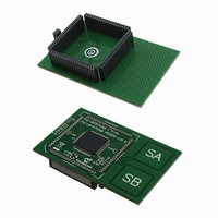
Manufacturer Part Number
MA180027
Description
MOD PLUG-IN PIC18F87K90 PICDEM2
Manufacturer
Microchip Technology
Series
PIC®r
Datasheet
1.MA180019.pdf
(66 pages)
Specifications of MA180027
Accessory Type
Plug-In Module (PIM) - PIC18F87K90
Interface Type
I2C, SPI
Operating Voltage
1.8 V to 5.5 V
Data Bus Width
8 bit
Maximum Operating Temperature
+ 125 C
Minimum Operating Temperature
- 40 C
Silicon Manufacturer
Microchip
Core Architecture
PIC
Core Sub-architecture
PIC18
Silicon Core Number
PIC18F
Silicon Family Name
PIC18F8xxx
For Use With/related Products
PICDEM LCD 2 Demonstration Board (DM163030)
Lead Free Status / RoHS Status
Lead free / RoHS Compliant
For Use With
DM163030 - KIT DEV PICDEM LCD2
Lead Free Status / Rohs Status
Lead free / RoHS Compliant
Available stocks
Company
Part Number
Manufacturer
Quantity
Price
Company:

Part Number:
MA180027
Manufacturer:
MICROCHIP
Quantity:
12 000


PICDEM™ LCD 2 Demonstration Kit User’s Guide
A.3
A.4
A.5
DS51662C-page 46
LED DISPLAY
CHARGE PUMP AND VLCAP
RESISTIVE LADDER VERSUS CHARGE PUMP
TABLE A-21:
Two green LEDs are connected to RC3 and RC4 of U1A through the J14 pins, 1, 2 and
7, 8 (outer ends), respectively.
One green LED is provided to determine whether there is power to the LCD 2
Demonstration Board (LED on) or not (LED off).
For charge pump mode operation in PIC18F85J90 and PIC18F87J90 devices, it is
required that RC3 and RC4 of U1A connect to charge pump capacitor C7 through the
J14 pins, 3, 4 and 5, 6 (inner pins), respectively.
The switch, S6, allows the connection of either the resistor ladder or the capacitors to
the BIAS pins to generate the BIAS voltages for the LCD operation. For the Charge
Pump mode operation in PIC18F85J90 and PIC18F87J90 devices, it is required that
the S6 switch is flipped towards C and the VLCAP is connected through the inner
jumpers of J14. For the resistor ladder, S6 must be flipped towards R. The R45
potentiometer controls the contrast to the LCD in the Resistive Ladder mode.
A.5.1
When jumper JP21 is on, the LCDBIAS0 is physically tied to ground. The jumper needs
to be on for PIC18F85J90 and PIC18F87J90 devices when the bias voltages are
generated through the resistor ladder.
Legend:
Note 1:
PIC16F917 Port
2:
3:
RA0
RA1
RA6
RA7
RB0
RB5
RB6
RB7
RC0
RC1
RC3
RC4
RC6
RC7
Unshaded cells indicate a perfect match between the PIM and the glass.
Shaded cells indicate the pins that are remapped to the corresponding pin on the PIM.
Jumper JP21
For the PIC18F85J90 and PIC18F87J90 PIM, the RG2 and RG3 pins are
connected to RC3 and RC4 of U1A, respectively.
For the PIC16F17 PIM, the RD1 and RD2 pins are connected to RC3 and
RC4 of U1A, respectively.
For the PIC18F8490 PIM, the RC3 and RD4 pins are connected to RC3
and RC4 of U1A, respectively
PIC16F917 PIN AND PORT COMPARISON
PIC16F917 Pin
T1OSCO
T1OSCI
VLCD1
VLCD2
SEG11
RX/DT
COM1
TX/CK
SEG6
AN0
AN1
RB0
RB6
RB7
T1OSCO
T1OSCI
ICE Pin
SEG11
SEG14
COM1
TX/CK
RX/DT
BIAS1
BIAS2
AN0
AN1
RB0
RB6
RB7
2010 Microchip Technology Inc.
ICE Port
RC0
RC1
RC6
RC7
RA0
RA1
RB0
RE4
RB6
RB7
RE0
RE1
RB4
RA4
Related parts for MA180027
Image
Part Number
Description
Manufacturer
Datasheet
Request
R

Part Number:
Description:
Manufacturer:
Microchip Technology Inc.
Datasheet:
Part Number:
Description:
Manufacturer:
Microchip Technology Inc.
Datasheet:
Part Number:
Description:
Manufacturer:
Microchip Technology Inc.
Datasheet:
Part Number:
Description:
Manufacturer:
Microchip Technology Inc.
Datasheet:
Part Number:
Description:
Manufacturer:
Microchip Technology Inc.
Datasheet:
Part Number:
Description:
Manufacturer:
Microchip Technology Inc.
Datasheet:
Part Number:
Description:
Manufacturer:
Microchip Technology Inc.
Datasheet:
Part Number:
Description:
Manufacturer:
Microchip Technology Inc.
Datasheet: