OCB100AZ TT Electronics/Optek Technology, OCB100AZ Datasheet - Page 2
OCB100AZ
Manufacturer Part Number
OCB100AZ
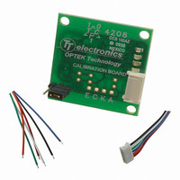
Description
BOARD CALIBR CIRCUIT PCB MNT
Manufacturer
TT Electronics/Optek Technology
Datasheet
1.OCB100AZ.pdf
(4 pages)
Specifications of OCB100AZ
Accessory Type
Interface Board
For Use With/related Products
Opto Isolators (Photo Couplers)
For Use With
365-1507 - KIT CALIBRATION CIRC OPTO ASSY
Lead Free Status / RoHS Status
Lead free / RoHS Compliant
Other names
365-1533
Available stocks
Company
Part Number
Manufacturer
Quantity
Price
Company:

Part Number:
OCB100AZ
Manufacturer:
TT Electronics/Optek Technolog
Quantity:
135


Automatic Calibration Circuitry
OCB 100 Series
Theory of operation:
The OCB100 series is designed to minimize the change of optical devices due to manufacturing variance. This
system can be used to calibrate either reflective or interruptive devices and provide a consistent output eliminating
the requirement to confirm either the LED drive resistance or Phototransistor Load Resistor to provide a consistent
output steady state condition. With the OCB100, the design engineer can narrow the expected startup output
state providing a device that will operate the same for years with the same startup state thus enhancing the
reliability and consistence of the system. Degradation of the LED or phototransistor is compensated for each time
the system is calibrated allowing the system to provide a known, consistent output level resulting in years of
consistent quality. The OCB100 series are designed to maintain the calibrated setting even if power is lost. This
allows faster startup without the need for calibration every time the device is initiated. The designer can initiate the
calibration procedure at any time by momentarily grounding J1-Pin-4 (green wire). This allows the device to be
remotely calibrated then mounted in the equipment.
The PCBoard has a set of shorting pins allowing the user to change the phototransistor load resistor. By arranging
the shorting bar to the appropriate location (see table), the load resistance can be changed from approximately
2.5K to 27 K Ω. Increasing the load resistor increases the sensitivity of the device.
When the “Calibrate” pin (#4) is momentarily grounded, the system begins its calibration process and raises the
current through the LED, from 0 mA to 14 mA, until the phototransistor reaches the preset calibration point. A
green calibration light will blink 3 times when the preset phototransistor output level is reached. At this time, the
LED drive current is locked and maintained until Reset/Clear pin is grounded. If for some reason, the LED drive
current reaches the maximum allowable value, a RED warning light will be turned on. During the calibration
process, remote monitoring of J1-Pin3 allows the designer to ensure the system is calibrated (this output should
be at the preset calibrated output level when the calibration procedure is completed). Adjusting the phototransistor
load resistor may allow the system to calibrate properly.
After the calibration process is complete, the device is ready for acknowledgement of a change in the signal. The
design engineer can monitor either the Analog Output (J1-Pin 5) or Logical Output (J1-Pin 2 or J1-Pin 3).
The Analog Output allows the design engineer to set any reference point to recognize an optical change for the
device being monitored. The Analog Output can be used with reflective devices to monitor small changes in the
distance from the device. The further the target is away from the device, the lower the reflected signal.
The Logical output will change state once the preset optical light condition is reached. The “Logic Out A” switches
when the optical signal increases above approximately 2/3 of V
signal decreases below approximately 1/3 of V
As with all optical devices, the switching condition is consistent with the phototransistor receiving a preset light
level. This switching position and light level may vary dependent on several possible factors such as:
The OCB100 PCBoard can be wired directly to any Optical device with an LED and Phototransistor.
Issue A
Page 2 of 4
•
•
•
•
•
•
•
•
•
10/08
Ambient light variation ((reduced or eliminated with periodic recalibration)
LED and phototransistor pair degradation (eliminated with periodic recalibration)
Contamination in front of either the LED or phototransistor (reduced or eliminated with periodic cleaning)
System power variation (reduced or eliminated with periodic recalibration)
Temperature changes (reduced or eliminated with periodic recalibration)
Interruptive devices / slotted switches / interruptive encoders
Reflective devices / reflective switches / reflective encoders
Specialty devices / fluid sensors
Etc.
OPTEK reserves the right to make changes at any time in order to improve design and to supply the best product possible.
Phone: (972) 323-2200 or (800) 341-4747
CC
.
CC
OPTEK Technology Inc. — 1645 Wallace Drive, Carrollton, Texas 75006
while “Logic Out B” switches when the optical
FAX: (972) 323-2396 visibleLED@optekinc.com www.optekinc.com
Related parts for OCB100AZ
Image
Part Number
Description
Manufacturer
Datasheet
Request
R

Part Number:
Description:
KIT CALIBRATION CIRC OPTO ASSY
Manufacturer:
TT Electronics/Optek Technology
Datasheet:

Part Number:
Description:
TRANSISTOR PNP GP HERMETIC SMD
Manufacturer:
TT Electronics/Optek Technology
Datasheet:
Part Number:
Description:
TRANSISTOR PNP GP HERMETIC SMD
Manufacturer:
TT Electronics/Optek Technology
Datasheet:
Part Number:
Description:
TRANSISTOR NPN GP HERMETIC SMD
Manufacturer:
TT Electronics/Optek Technology
Datasheet:

Part Number:
Description:
LED IR 880NM FLAT LENS 0805 SMD
Manufacturer:
TT Electronics/Optek Technology
Datasheet:

Part Number:
Description:
LED IR 880NM 1.9MM LENS AXIAL
Manufacturer:
TT Electronics/Optek Technology
Datasheet:

Part Number:
Description:
LED IR 890NM PLSTC NARROW TO-46
Manufacturer:
TT Electronics/Optek Technology
Datasheet:
Part Number:
Description:
LED IR 5MM 890NM PLASTIC
Manufacturer:
TT Electronics/Optek Technology
Datasheet:
Part Number:
Description:
LED IR 890NM PLSTC NARROW TO-46
Manufacturer:
TT Electronics/Optek Technology
Datasheet:
Part Number:
Description:
LED IR 5MM 890NM PLASTIC
Manufacturer:
TT Electronics/Optek Technology
Datasheet:
Part Number:
Description:
TRANSISTOR PNP GP HERMETIC SMD
Manufacturer:
TT Electronics/Optek Technology
Datasheet:
Part Number:
Description:
TRANSISTOR PNP GP HERMETIC SMD
Manufacturer:
TT Electronics/Optek Technology
Datasheet:
Part Number:
Description:
TRANSISTOR NPN GP HERMETIC SMD
Manufacturer:
TT Electronics/Optek Technology
Datasheet:
Part Number:
Description:
LED IR 880NM FLAT LENS 0805 SMD
Manufacturer:
TT Electronics/Optek Technology
Datasheet:
Part Number:
Description:
TRANSISTR MOS ENHANCE N-CHAN SMD
Manufacturer:
TT Electronics/Optek Technology
Datasheet: