C8051F700-TB Silicon Laboratories Inc, C8051F700-TB Datasheet
C8051F700-TB
Manufacturer Part Number
C8051F700-TB
Description
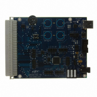
BOARD PROTOTYPE WITH C8051F700
Manufacturer
Silicon Laboratories Inc
Datasheets
1.C8051F700-TB.pdf
(1 pages)
2.C8051F700-TB.pdf
(306 pages)
3.C8051F700-TB.pdf
(18 pages)
Specifications of C8051F700-TB
Accessory Type
Target Board
Processor To Be Evaluated
C8051F700
Processor Series
C8051F7xx
Interface Type
USB
Operating Supply Voltage
7 V to 15 V
Lead Free Status / RoHS Status
Lead free / RoHS Compliant
For Use With/related Products
C8051F7xx
Lead Free Status / Rohs Status
Lead free / RoHS Compliant
Other names
336-1637
C8051F700
C8051F700
High-Speed 8051 µC Core
-
-
Memory
-
-
-
-
Analog Peripherals
10-Bit Analog to Digital Converter (‘F700)
-
-
-
-
-
Comparator
-
-
Capacitive Touch Sense
-
-
-
-
-
Precision Mixed Signal
Pipelined instruction architecture; executes 70% of instructions in 1 or 2
system clocks
Up to 25 MIPS throughput with 25 MHz system clock
15 kB Flash; in-application programmable in 512-byte sectors
32 bytes Data EEPROM with 100,000 cycle read/write endurance
512 bytes data RAM
External parallel data memory interface
Up to 500 ksps
16 external inputs
On-chip voltage reference (may use VDD or external voltage)
Built-in temperature sensor
External conversion start input option
Programmable hysteresis and response time
Configurable as interrupt or reset source
16-bit capacitance-to-Digital Converter
Superior Noise Immunity and fast 40us aquisition time
Up to 32 external inputs
Auto-scan and compare
Auto-accumulate 4x, 8x, and 16x samples
C2CK/RST
GND
VDD
Peripheral Power
Programming
C2D
Power On
Hardware
Regulator
Debug /
Reset
XTAL1
XTAL2
Reset
Core Power
Precision
Oscillator
External
Internal
Circuit
Controller Core
15 kB Flash Memory
System Clock
25 MIPS, 15 kB Flash, 10-Bit ADC, 64-Pin Mixed-Signal MCU
Clock
Configuration
32 Bytes EEPROM
CIP-51 8051
256 Byte XRAM
256 Byte RAM
Copyright © 2009 by Silicon Laboratories
SYSCLK
SFR
Bus
VDD
Digital Peripherals
Up to 54 Port I/O with high sink current
-
-
-
Serial Communications
-
-
-
User Programmable Timing Functions
-
-
-
Clock Sources
-
-
-
Supply Voltage: 1.8 to 3.3 V
-
Temperature Range: –40 to +85 °C
TQFP-64 Package
Timers 0,
Timer 3 /
10-bit
500 ksps
ADC
SMBus
External Memory
UART
1, 2, 3
Digital Peripherals
WDT
RTC
PCA
Flexible configuration using digital crossbar
Many can be configured for analog or digital function
Every pin can be optimized for its best use
HW enhanced UART
SMBus
Enhanced SPI
Four general purpose 16-bit counter/timers
16-bit programmable counter array (PCA) with three capture/compare
modules and enhanced PWM capability
Real-time clock mode using enhanced timer and crystal
Calibrated Internal programmable oscillator
External oscillator: Crystal, RC, C, or Clock
Can switch between clock sources on-the-fly
Built-in voltage supply monitor
Port I/O Configuration
SPI
•
•
•
Crossbar Control
Interface
Address
Analog Peripherals
Control
Data
TM
Calibrated to 2% accuracy over temp and Vdd
24.5 MHz to allow max speed CPU operation
Supports crystal-less UART operation
VREF
Capacitive
Sense
A
M
U
X
(I
2
C compatible)
Crossbar
Decoder
Priority
TM
VDD
Temp Sensor
(‘F700 Only)
P4 / P3
P6
P5
Comparator
Drivers
Drivers
Drivers
Drivers
Drivers
Drivers
Drivers
Port 0
Port 1
Port 2
Port 3
Port 4
Port 5
Port 6
C8051F700/1
+
-
. . .
. . .
. . .
. . .
. . .
P0.0 / VREF
P0.1 / AGND
P0.2 / XTAL1
P0.3 / XTAL2
P0.4
P0.5
P0.6
P0.7
P1.0
P1.1
P1.2
P1.3
P1.4
P1.5
P1.6
P1.7
P2.0
P2.7
P3.0
P3.7
P4.0
P4.7
P5.0
P5.7
P6.0
P6.5
2.16.2009
Related parts for C8051F700-TB
Image
Part Number
Description
Manufacturer
Datasheet
Request
R

Part Number:
Description:
SMD/C�/SINGLE-ENDED OUTPUT SILICON OSCILLATOR
Manufacturer:
Silicon Laboratories Inc
Part Number:
Description:
Manufacturer:
Silicon Laboratories Inc
Datasheet:
Part Number:
Description:
N/A N/A/SI4010 AES KEYFOB DEMO WITH LCD RX
Manufacturer:
Silicon Laboratories Inc
Datasheet:
Part Number:
Description:
N/A N/A/SI4010 SIMPLIFIED KEY FOB DEMO WITH LED RX
Manufacturer:
Silicon Laboratories Inc
Datasheet:
Part Number:
Description:
N/A/-40 TO 85 OC/EZLINK MODULE; F930/4432 HIGH BAND (REV E/B1)
Manufacturer:
Silicon Laboratories Inc
Part Number:
Description:
EZLink Module; F930/4432 Low Band (rev e/B1)
Manufacturer:
Silicon Laboratories Inc
Part Number:
Description:
I�/4460 10 DBM RADIO TEST CARD 434 MHZ
Manufacturer:
Silicon Laboratories Inc
Part Number:
Description:
I�/4461 14 DBM RADIO TEST CARD 868 MHZ
Manufacturer:
Silicon Laboratories Inc
Part Number:
Description:
I�/4463 20 DBM RFSWITCH RADIO TEST CARD 460 MHZ
Manufacturer:
Silicon Laboratories Inc
Part Number:
Description:
I�/4463 20 DBM RADIO TEST CARD 868 MHZ
Manufacturer:
Silicon Laboratories Inc
Part Number:
Description:
I�/4463 27 DBM RADIO TEST CARD 868 MHZ
Manufacturer:
Silicon Laboratories Inc
Part Number:
Description:
I�/4463 SKYWORKS 30 DBM RADIO TEST CARD 915 MHZ
Manufacturer:
Silicon Laboratories Inc
Part Number:
Description:
N/A N/A/-40 TO 85 OC/4463 RFMD 30 DBM RADIO TEST CARD 915 MHZ
Manufacturer:
Silicon Laboratories Inc
Part Number:
Description:
I�/4463 20 DBM RADIO TEST CARD 169 MHZ
Manufacturer:
Silicon Laboratories Inc