MCP46XXDM-PTPLS Microchip Technology, MCP46XXDM-PTPLS Datasheet - Page 21
MCP46XXDM-PTPLS
Manufacturer Part Number
MCP46XXDM-PTPLS
Description
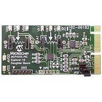
BOARD PICTAIL DIGI POT MCP4XXX
Manufacturer
Microchip Technology
Series
PICtail™ Plusr
Datasheet
1.MCP46XXDM-PTPLS.pdf
(44 pages)
Specifications of MCP46XXDM-PTPLS
Main Purpose
Digital Potentiometer
Embedded
No
Utilized Ic / Part
MCP46xx
Primary Attributes
1 Dual Pot, 10k Ohms, 257 Taps, I²C Interface
Secondary Attributes
2.7 ~ 5.5 V, 150 ppm/°C
Silicon Manufacturer
Microchip
Silicon Core Number
MCP4631, MCP4632, MCP4641, MCP4642, MCP4651, MCP4652, MCP4661, MCP4662
Kit Contents
Board
Lead Free Status / RoHS Status
Lead free / RoHS Compliant


© 2009 Microchip Technology Inc.
2.4.1.3
The Explorer 16 Development Board firmware contains two programs. The program
selected is determined after a reset (including the Power-on reset) by the state of the
S3 switch. The programs are:
1. Wiper 1 Saw Wave (Switch S3 not depressed).
2. Increment / Decrement with High Voltage Write to Non-Volatile Wiper 1 Register
Table 2-2 shows the sequence of steps to demonstrate the MCP46XXDM-PTPLS
board with the Explorer 16 Development Board.
Figure 2-6 shows the expected output waveform for Program #1 (Wiper 1 Saw Wave)
as well as the voltage levels and ranges of the four signals. Figure 2-7 shows an
example waveforms for the High Voltage Write Command for the SDA, SCL, and HVC
signals.
TABLE 2-2:
1a
1b
2a
2b
3
4
5
6
7
Note 1:
Step
(Switch S3 depressed).
Turn on the oscilloscope and configure it as
follows:
• Channel 1, 2, 3, and 4 @ 5V/Division
• Channel 1 to 4 have the same ground
Configure the oscilloscope as follows:
• Time-base = 10 ms/Division
Configure the MCP46XXDM-PTPLS to the
jumper settings shown in
On the Explorer 16 Development Board,
remove the shunt on JP2 (near the indicator
LEDs).
Insert the MCP46XXDM-PTPLS board into the
Explorer 16 Development Board J5 header
(see
Daughter Board to J5 Header.
Connect the oscilloscope probes as follows:
• Channel 1 to the CS Pin of Header J1
• Channel 2 to the SDA Pin of Header J2
• Channel 3 to the SCL Pin of Header J2
• Channel 4 to the VW1 Pad
Power up the programmed Explorer 16
Development Board and depress and release
the MCLR push button.
Depress the Explorer 16 Development Board’s
S3 push button.
Depress and release the Explorer 16
Development Board’s MCLR push button.
reference point
(see
(HVC signal of MCP4661)
The SDA and SCL signals go from V
operating at 3.3V. The VW1 signals go from V
DEMO STEPS
Figure 2-5
Figure 2-6
DEMO STEPS USING THE PICDEM HPC EXPLORER DEMO
BOARD
). Ensure proper orientation of
for scope details)
Action
Figure 2-4
.
SS
to approximately 3.3V due to the PIC24
—
—
—
The LEDs are disabled (no longer
connected to ground).
—
—
Program 1 is now selected.
Output waveform should look similar
to
voltage levels/ranges of the four
signals.
(Note 1)
—
—
SS
Figure 2-6
to approximately 5V.
. Ensure to verify
Result
DS51804A-page 17
Related parts for MCP46XXDM-PTPLS
Image
Part Number
Description
Manufacturer
Datasheet
Request
R

Part Number:
Description:
Manufacturer:
Microchip Technology Inc.
Datasheet:
Part Number:
Description:
Manufacturer:
Microchip Technology Inc.
Datasheet:
Part Number:
Description:
Manufacturer:
Microchip Technology Inc.
Datasheet:
Part Number:
Description:
Manufacturer:
Microchip Technology Inc.
Datasheet:
Part Number:
Description:
Manufacturer:
Microchip Technology Inc.
Datasheet:
Part Number:
Description:
Manufacturer:
Microchip Technology Inc.
Datasheet:
Part Number:
Description:
Manufacturer:
Microchip Technology Inc.
Datasheet:
Part Number:
Description:
Manufacturer:
Microchip Technology Inc.
Datasheet: