KIT33880DWBEVB Freescale Semiconductor, KIT33880DWBEVB Datasheet - Page 8
KIT33880DWBEVB
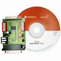
Manufacturer Part Number
KIT33880DWBEVB
Description
KIT EVAL FOR MC33880 8X SW W/SPI
Manufacturer
Freescale Semiconductor
Specifications of KIT33880DWBEVB
Main Purpose
Power Management, High & Low Side Driver (Internal FET)
Embedded
No
Utilized Ic / Part
MC33880
Primary Attributes
8 Configurable High/Low FETs, 5.5 ~ 24.5V, 0.8 ~ 2A, 0.55 Ohm
Secondary Attributes
SPI Interface, Reverse Battery, Temperature, Short Circuit, Current Limit Protection
Lead Free Status / RoHS Status
Contains lead / RoHS non-compliant


Table 5. Dynamic Electrical Characteristics
noted. Typical values, where applicable, reflect the parameter’s approximate average value with V
8
POWER OUTPUT TIMING
DIGITAL INTERFACE TIMING
Notes
33880
ELECTRICAL CHARACTERISTICS
DYNAMIC ELECTRICAL CHARACTERISTICS
Output Slew Rate Low-Side Configuration
Output Slew Rate Low-Side Configuration
Output Slew Rate High-Side Configuration
Output Slew Rate High-Side Configuration
Output Turn ON Delay Time, High-Side and Low-Side Configuration
Output Turn OFF Delay Time, High-Side and Low-Side Configuration
Output Fault Delay Time
Recommended Frequency of SPI Operation
Required Low State Duration on V
Falling Edge of CS to Rising Edge of SCLK (Required Setup Time)
Falling Edge of SCLK to Rising Edge of CS (Required Setup Time)
DI to Falling Edge of SCLK (Required Setup Time)
Falling Edge of SCLK to DI (Required Hold Time)
DI, CS, SCLK Signal Rise Time
DI, CS, SCLK Signal Fall Time
Time from Falling Edge of CS to DO Low Impedance
Time from Rising Edge of CS to DO High Impedance
Time from Rising Edge of SCLK to DO Data Valid
14.
15.
16.
17.
18.
19.
20.
21.
Characteristics noted under conditions 4.75 V ≤ V
R
R
R
R
V
L
L
L
L
DD
= 620 Ω
= 620 Ω
= 620 Ω
= 620 Ω
Output Rise and Fall time respectively measured across a 620 Ω resistive load at 10 to 90 percent and 90 to 10 percent voltage points.
Output turn ON and OFF delay time measured from 50 percent rising edge of
Duration of fault before fault bit is set. Duration between access times must be greater than 300 μs to read faults.
This parameter is guaranteed by design but is not production tested.
Rise and Fall time of incoming DI,
Time required for output status data to be available for use at DO pin.
Time required for output status data to be terminated at DO pin
Time required to obtain valid data out from DO following the rise of SCLK.
≤ 0.2 V
(16)
Characteristic
(18)
(18)
DD
for Reset
CS
DYNAMIC ELECTRICAL CHARACTERISTICS
(14)
(14)
(14)
(14)
, and SCLK signals suggested for design consideration to prevent the occurrence of double pulsing.
(17)
(21)
(19)
(20)
DD
≤ 5.25 V, 9.0 V ≤ V
(15)
(15)
t
t
Symbol
t
DLY(OFF)
t
DI(HOLD)
DLY(ON)
t
t
t
DO(DIS)
DO(EN)
t
RESET
t
t
PWR
FAULT
t
t
DI(su)
VALID
LEAD
t
R(DI)
F(DI)
LAG
t
t
CS
t
t
–
R
F
R
F
to 90 and 10 percent of initial voltage.
≤ 16 V, -40°C ≤ T
Min
100
100
0.1
0.1
0.1
0.1
1.0
1.0
50
16
20
–
–
–
–
–
–
–
Analog Integrated Circuit Device Data
C
Typ
PWR
0.5
0.5
0.3
0.3
4.0
4.0
5.0
5.0
15
30
25
≤ 125°C unless otherwise
–
–
–
–
–
–
–
Freescale Semiconductor
= 13 V, T
Max
100
300
1.2
1.2
1.2
1.2
6.0
50
10
60
60
60
–
–
–
–
–
–
A
= 25°C.
Unit
V/μs
V/μs
V/μs
V/μs
MHz
μs
μs
μs
μs
ns
ns
ns
ns
ns
ns
ns
ns
ns
Related parts for KIT33880DWBEVB
Image
Part Number
Description
Manufacturer
Datasheet
Request
R

Part Number:
Description:
Manufacturer:
Freescale Semiconductor, Inc
Datasheet:
Part Number:
Description:
Manufacturer:
Freescale Semiconductor, Inc
Datasheet:
Part Number:
Description:
Manufacturer:
Freescale Semiconductor, Inc
Datasheet:
Part Number:
Description:
Manufacturer:
Freescale Semiconductor, Inc
Datasheet:
Part Number:
Description:
Manufacturer:
Freescale Semiconductor, Inc
Datasheet:
Part Number:
Description:
Manufacturer:
Freescale Semiconductor, Inc
Datasheet:
Part Number:
Description:
Manufacturer:
Freescale Semiconductor, Inc
Datasheet:
Part Number:
Description:
Manufacturer:
Freescale Semiconductor, Inc
Datasheet:
Part Number:
Description:
Manufacturer:
Freescale Semiconductor, Inc
Datasheet:
Part Number:
Description:
Manufacturer:
Freescale Semiconductor, Inc
Datasheet:
Part Number:
Description:
Manufacturer:
Freescale Semiconductor, Inc
Datasheet:
Part Number:
Description:
Manufacturer:
Freescale Semiconductor, Inc
Datasheet:
Part Number:
Description:
Manufacturer:
Freescale Semiconductor, Inc
Datasheet:
Part Number:
Description:
Manufacturer:
Freescale Semiconductor, Inc
Datasheet:
Part Number:
Description:
Manufacturer:
Freescale Semiconductor, Inc
Datasheet: