NBC124XXEVB ON Semiconductor, NBC124XXEVB Datasheet - Page 7
NBC124XXEVB
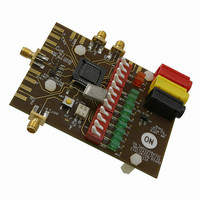
Manufacturer Part Number
NBC124XXEVB
Description
EVAL BOARD FOR NBC124XX
Manufacturer
ON Semiconductor
Datasheets
1.NBC12439FAR2G.pdf
(21 pages)
2.NBC12429FAR2G.pdf
(22 pages)
3.NBC12430FAR2G.pdf
(20 pages)
Specifications of NBC124XXEVB
Design Resources
NBC124XXEVB Gerber Files
Main Purpose
Timing, PLL
Embedded
No
Utilized Ic / Part
NBC12429, NBC12430, NBC12439
Primary Attributes
DIP Switch Controlled M & N Logic
Secondary Attributes
Push Button or Externally Controlled P_Load
Technology Type
Evaluation Board
Lead Free Status / RoHS Status
Lead free / RoHS Compliant
For Use With/related Products
NBC124XX
Other names
NBC124XXEVBOS


NOTE: Device will meet the specifications after thermal equilibrium has been established when mounted in a test socket or printed circuit
6. 10 MHz is the maximum frequency to load the feedback divide registers. S_CLOCK can be switched at higher frequencies when used as
7. F
8. Maximum frequency on FREF_EXT is a function of setting the appropriate M counter value for the VCO to operate within the valid range
Table 8. AC CHARACTERISTICS
(Note 7)
F
F
t
t
t
t
t
tpw
DCO
t
LOCK
jitter(pd)
jitter(cyc−cyc)
s
h
r
, t
MAXI
MAXO
a test clock in TEST_MODE 6.
of 400 MHz v f
Symbol
f
OUT/
MIN
board with maintained transverse airflow greater than 500 lfpm. Electrical parameters are guaranteed only over the declared
operating temperature range. Functional operation of the device exceeding these conditions is not implied. Device specification limit
values are applied individually under normal operating conditions and not valid simultaneously.
F
OUT
and TEST outputs are terminated through a 50 W resistor to V
Maximum Input Frequency
Maximum Output Frequency
Maximum PLL Lock Time
Period Jitter (RMS)
Cycle−to−Cycle Jitter (Peak−to−Peak)
Setup Time
Hold Time
Minimum Pulse Width
Output Duty Cycle
Output Rise/Fall
VCO
v 800 MHz. (See Table 11)
Characteristic
(V
CC
S_CLOCK to S_LOAD
S_DATA to S_CLOCK
S_DATA to S_CLOCK
= 3.135 V to 5.25 V ± 5%; T
FREF_EXT (Note 8)
M, N to P_LOAD
M, N to P_LOAD
XTAL Oscillator
VCO (Internal)
S_CLOCK
http://onsemi.com
S_LOAD
P_LOAD
F
F
(1s)
(8s)
OUT
OUT
7
(Note 6)
50 MHz v f
100 MHz v f
50 MHz v f
100 MHz v f
20%−80%
A
= 0°C to 70°C (NBC12430), T
CC
Condition
− 2.0 V.
OUT
OUT
OUT
OUT
< 100 MHz
< 100 MHz
< 800 MHz
< 800 MHz
A
47.5
Min
400
175
= −40°C to 85°C (NBC12430A))
10
10
50
20
20
20
20
20
50
50
"40
"20
Max
52.5
100
800
800
425
10
20
10
8
5
MHz
MHz
Unit
ms
ps
ps
ns
ns
ns
ps
%
Related parts for NBC124XXEVB
Image
Part Number
Description
Manufacturer
Datasheet
Request
R

Part Number:
Description:
ON Semiconductor [VOLTAGE REGULATOR]
Manufacturer:
ON Semiconductor
Datasheet:
Part Number:
Description:
357-036-542-201 CARDEDGE 36POS DL .156 BLK LOPRO
Manufacturer:
ON Semiconductor
Datasheet:
Part Number:
Description:
357-036-542-201 CARDEDGE 36POS DL .156 BLK LOPRO
Manufacturer:
ON Semiconductor
Datasheet:
Part Number:
Description:
357-036-542-201 CARDEDGE 36POS DL .156 BLK LOPRO
Manufacturer:
ON Semiconductor
Datasheet:
Part Number:
Description:
357-036-542-201 CARDEDGE 36POS DL .156 BLK LOPRO
Manufacturer:
ON Semiconductor
Datasheet:
Part Number:
Description:
357-036-542-201 CARDEDGE 36POS DL .156 BLK LOPRO
Manufacturer:
ON Semiconductor
Datasheet:
Part Number:
Description:
357-036-542-201 CARDEDGE 36POS DL .156 BLK LOPRO
Manufacturer:
ON Semiconductor
Datasheet:
Part Number:
Description:
357-036-542-201 CARDEDGE 36POS DL .156 BLK LOPRO
Manufacturer:
ON Semiconductor
Datasheet:
Part Number:
Description:
357-036-542-201 CARDEDGE 36POS DL .156 BLK LOPRO
Manufacturer:
ON Semiconductor
Datasheet:
Part Number:
Description:
357-036-542-201 CARDEDGE 36POS DL .156 BLK LOPRO
Manufacturer:
ON Semiconductor
Datasheet:
Part Number:
Description:
357-036-542-201 CARDEDGE 36POS DL .156 BLK LOPRO
Manufacturer:
ON Semiconductor
Datasheet:
Part Number:
Description:
Manufacturer:
ON Semiconductor
Datasheet:
Part Number:
Description:
Manufacturer:
ON Semiconductor
Datasheet:
Part Number:
Description:
Manufacturer:
ON Semiconductor
Datasheet: