VSUPEV2 Microchip Technology, VSUPEV2 Datasheet - Page 21
VSUPEV2
Manufacturer Part Number
VSUPEV2
Description
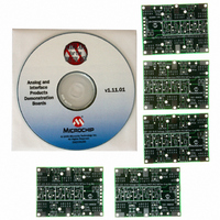
BOARD EVAL FOR MCP4022,4023,4024
Manufacturer
Microchip Technology
Specifications of VSUPEV2
Main Purpose
Power Management, Power Supply Supervisor/Tracker/Sequencer
Embedded
No
Utilized Ic / Part
SOT-23-5, SOT-23-6 Package
Primary Attributes
Voltage Detector & Supervisor
Secondary Attributes
5 Boards & 3 IC's Included
Processor To Be Evaluated
SOT23-5/6
Lead Free Status / RoHS Status
Lead free / RoHS Compliant
Lead Free Status / RoHS Status
Lead free / RoHS Compliant, Lead free / RoHS Compliant


2.5
FIGURE 2-5:
© 2006 Microchip Technology Inc.
Pin Number of that
Footprint Version
(1, 2, 3, 4, 5 or 6)
Footprint Version
(A, B, C, D or E)
C5C
VOLTAGE SUPERVISOR/VOLTAGE DETECTOR CIRCUITS
V
TP3A
SS
A B C
2 6 2
R2C
R3C
Currently, the voltage detectors/voltage supervisors use either footprint option A or
footprint option D.
2.5.1
Using the TC53C or TC54VC, no passive components would be required and the
device V
Using the TC53N or TC54VN, an external pull-up resistor is required. This resistor
would be installed in the R2A location and the device V
D1 pad.
The TC52 is a dual-channel voltage detector. This means that the device has a V
and a V
Locations R2A and R2E should be installed with 47 kΩ resistors.
Detect voltage 2 (V
typically used to indicate a low-power situation, with V
system. Typically, a 0.1 µF capacitor would be on the V
location).
Power supply filtering may be required, so a 0.1 µF capacitor is suggested in the C4
location.
Voltage Supervisor Circuit using Option D Footprint.
D
3
E
2
OUT2
OUT
A B C D E
5 5 5 5 6
R1C
Option D Circuit
C4
could be monitored on the D1 pad.
output. Both outputs are open-drain and require a pull-up resistor.
3
1
2
Option D
S1
OUT2
U4
A B C
3 3 3
) is lower than detect voltage 1 (V
Footprint Option/Pin Number
Combination (Pad D5)
(MR
5
4
V
IN+
TP 3
)
—
D
E
3
C5A
C5E
C5D
TP1A
TP4A
TP5A
C5F
R2A
R3A
R2E
R3E
R2D
R3D
OUT2
OUT
OUT2
OUT1
R1A
could be monitored on the
being used to reset the
R1D
pin (installed in the C5E
R1E
). Therefore, V
S2
A B C
5 5 5
A B C
4 4 4
A B C
6 2 1
A B C
1 1 6
DS51527B-page 17
(V
V
IN+
OUT
V
TP 1
(WDI
(WDI
V
V
DD
)
IN–
IN–
D
D
TP 5
5
4
D
D
2
1
OUT1
)
TP 4
)
E
6
E
4
E
5
E
1
OUT1
is
Related parts for VSUPEV2
Image
Part Number
Description
Manufacturer
Datasheet
Request
R

Part Number:
Description:
Manufacturer:
Microchip Technology Inc.
Datasheet:
Part Number:
Description:
Manufacturer:
Microchip Technology Inc.
Datasheet:
Part Number:
Description:
Manufacturer:
Microchip Technology Inc.
Datasheet:
Part Number:
Description:
Manufacturer:
Microchip Technology Inc.
Datasheet:
Part Number:
Description:
Manufacturer:
Microchip Technology Inc.
Datasheet:
Part Number:
Description:
Manufacturer:
Microchip Technology Inc.
Datasheet:
Part Number:
Description:
Manufacturer:
Microchip Technology Inc.
Datasheet:
Part Number:
Description:
Manufacturer:
Microchip Technology Inc.
Datasheet: