MXSIGDM Microchip Technology, MXSIGDM Datasheet - Page 20
MXSIGDM
Manufacturer Part Number
MXSIGDM
Description
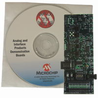
BOARD DEMO PICTAIL MIXED SIGNAL
Manufacturer
Microchip Technology
Series
PICtail™r
Datasheet
1.MXSIGDM.pdf
(54 pages)
Specifications of MXSIGDM
Main Purpose
Mixed Signal for MCU: ADC, DAC,
Embedded
Yes, MCU, 8-Bit
Utilized Ic / Part
TX132x,MCP330x,320x,494x,3221,3201,1525,1541
Primary Attributes
3 ADCs, 3 DACs, 2 Voltage References, 5V LDO
Secondary Attributes
DIP Switches, 2 LEDs, PIC16F767
Processor To Be Evaluated
TC132x, MCP330x, MCP320x, MCP492x, MCP3221, MCP3021, MCP15x
Interface Type
I2C, SPI
Lead Free Status / RoHS Status
Contains lead / RoHS non-compliant
Lead Free Status / RoHS Status
Lead free / RoHS Compliant, Contains lead / RoHS non-compliant


DS51523A-page 16
2.4.4
Jumper JP2 is located in the center of the board above JP1. JP2 consists of three pairs
of jumper pins. The lower two pins are connected to A
connected to V
Appendix A. “Schematics and Layouts”.
If the user would like to read Microchip’s MCP492X or MCP482X DAC A output with
either the MCP3302 or MCP3204, place a jumper from one of the middle two pins to
either of the outer pins, depending on which ADC input channel you are using.
2.4.5
Jumper JP3 is located in the center of the board just above the 8-pin, dual op amp
MCP617 and to the right of the SMA connector’s footprint. JP3 consists of three pairs
of jumper pins. The lower two pins are connected to A
connected to V
Appendix A. “Schematics and Layouts” to view the schematic.
If the user would like to read Microchip’s MCP492X or MCP482X DAC B output with
either the MCP3302 or MCP3204, place a jumper from one of the middle two pins to
either of the outer pins, depending on which ADC input channel you are using.
2.4.6
Jumper JP4 is located in the center of the board, farthest away from the PICmicro
microcontroller and its MPLAB ICD 2 connector. JP4 consists of three pairs of jumper
pins. The lower two pins are connected to the MCP1541’s 4.1V V
two pins are connected to the REF198G’s 4.1V V
NOT connected, similar to J1, J2 or J3. The middle left pin selects the V
source while the middle right pin selects the V
Appendix A. “Schematics and Layouts”.
If the user employs the REF19G as the V
TC132X DACs, a jumper connecting the top right pin with the middle right pin is
required. If the user would like to use the MCP1541 as the V
MCP492X, MCP482X or TC132X DACs, a jumper connecting the bottom right pin with
the middle right pin is required.
If the user employs the REF19G as the V
MCP3204 or PIC16F767 ADCs, a jumper connecting the top right pin with the middle
right pin is required. If the user employs the MCP1541 as the V
Microchip’s MCP492X, MCP482X or TC132X DACs, a jumper connecting the bottom
right pin with the middle right pin is required.
Note:
Note:
Note:
Jumper JP2 Selection
Jumper JP3 Selection
Jumper JP4 Selection
The default firmware Mode0101 requires JP3 to be connected to A
read V
The default firmware requires a V
modes.
The default firmware Modes0100, 0101, 1100 and 1101 require V
to be selected in order to function.
OUTA
OUTB
OUTB
. The top two pins are connected to A
. The top two pins are connected to A
with the MCP3302 or MCP3204.
REF
REF
REF_DAC
REF_DAC
source for Microchip’s MCP492X or
source for Microchip’s MCP3302,
REF
jumper to function for almost all
output. The middle two pins are
IN_A
IN_D
source. Refer to Figure 2-2 and
IN_C
IN_B
. The middle two pins are
. The middle two pins are
2004 Microchip Technology Inc.
REF
. Refer to Figure 2-2 and
. Refer to Figure 2-2 and
REF
source for Microchip’s
REF
source for
output. The top
REF_ADC
REF_ADC
IN_B
to
Related parts for MXSIGDM
Image
Part Number
Description
Manufacturer
Datasheet
Request
R

Part Number:
Description:
Manufacturer:
Microchip Technology Inc.
Datasheet:
Part Number:
Description:
Manufacturer:
Microchip Technology Inc.
Datasheet:
Part Number:
Description:
Manufacturer:
Microchip Technology Inc.
Datasheet:
Part Number:
Description:
Manufacturer:
Microchip Technology Inc.
Datasheet:
Part Number:
Description:
Manufacturer:
Microchip Technology Inc.
Datasheet:
Part Number:
Description:
Manufacturer:
Microchip Technology Inc.
Datasheet:
Part Number:
Description:
Manufacturer:
Microchip Technology Inc.
Datasheet:
Part Number:
Description:
Manufacturer:
Microchip Technology Inc.
Datasheet: