MCP3421DM-BFG Microchip Technology, MCP3421DM-BFG Datasheet - Page 11
MCP3421DM-BFG
Manufacturer Part Number
MCP3421DM-BFG
Description
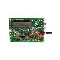
BOARD DEMO FOR MCP3421
Manufacturer
Microchip Technology
Datasheets
1.MCP3421A2T-ECH.pdf
(42 pages)
2.MCP3421DM-BFG.pdf
(26 pages)
3.MCP3421A0T-ECH.pdf
(30 pages)
Specifications of MCP3421DM-BFG
Main Purpose
Power Management, Battery Gauge
Utilized Ic / Part
MCP3421
Processor To Be Evaluated
MCP3421
Lead Free Status / RoHS Status
Lead free / RoHS Compliant
Secondary Attributes
-
Embedded
-
Primary Attributes
-
Lead Free Status / RoHS Status
Lead free / RoHS Compliant, Lead free / RoHS Compliant


5.2
The MCP3421 has an 8-bit wide configuration register
to select for: PGA gain, conversion rate, and conver-
sion mode. This register allows the user to change the
operating condition of the device and check the status
of the device operation. The user can rewrite the
configuration byte any time during the device
operation. Register 5-1
register bits.
REGISTER 5-1:
© 2007 Microchip Technology Inc.
bit 7
* Default Configuration after Power-On Reset
Legend:
R = Readable bit
-n = Value at POR
bit 7
bit 6-5
bit 4
bit 3-2
bit 1-0
R/W-1
RDY
1 *
Configuration Register
RDY: Ready Bit
This bit is the data ready flag. In read mode, this bit indicates if the output register has been updated
with a new conversion. In One-Shot Conversion mode, writing this bit to “1” initiates a new conversion.
Reading RDY bit with the read command:
1 = Output register has not been updated.
0 = Output register has been updated with the latest conversion data.
Writing RDY bit with the write command:
Continuous Conversion mode: No effect
One-Shot Conversion mode:
1 = Initiate a new conversion.
0 = No effect.
C1-C0: Channel Selection Bits
These are the Channel Selection bits, but not used in the MCP3421 device.
O/C: Conversion Mode Bit
1 = Continuous Conversion Mode. Once this bit is selected, the device performs data conversions
0 = One-Shot Conversion Mode. The device performs a single conversion and enters a low power
S1-S0: Sample Rate Selection Bit
00 =
01 =
10 =
11 =
G1-G0: PGA Gain Selector Bits
00 =
01 =
10 =
11 =
R/W-0
continuously.
standby mode until it receives another write/read command.
C1
0 *
CONFIGURATION REGISTER
240 SPS (12 bits),
60 SPS (14 bits),
15 SPS (16 bits),
3.75 SPS (18 bits)
1 V/V,
2 V/V,
4 V/V,
8 V/V
shows the configuration
W = Writable bit
‘1’ = Bit is set
R/W-0
C0
0 *
R/W-1
O/C
1 *
‘0’ = Bit is cleared
U = Unimplemented bit, read as ‘0’
R/W-0
S1
0 *
R/W-0
S0
0 *
x = Bit is unknown
R/W-0
MCP3421
G1
0 *
DS22003D-page 11
R/W-0
G0
0 *
bit 0
Related parts for MCP3421DM-BFG
Image
Part Number
Description
Manufacturer
Datasheet
Request
R

Part Number:
Description:
18-Bit Analog-to-Digital Converter with I2C Interface and On-Board Reference
Manufacturer:
Microchip Technology
Datasheet:

Part Number:
Description:
Manufacturer:
Microchip Technology Inc.
Datasheet:
Part Number:
Description:
Manufacturer:
Microchip Technology Inc.
Datasheet:
Part Number:
Description:
Manufacturer:
Microchip Technology Inc.
Datasheet:
Part Number:
Description:
Manufacturer:
Microchip Technology Inc.
Datasheet:
Part Number:
Description:
Manufacturer:
Microchip Technology Inc.
Datasheet:
Part Number:
Description:
Manufacturer:
Microchip Technology Inc.
Datasheet:
Part Number:
Description:
Manufacturer:
Microchip Technology Inc.
Datasheet:
Part Number:
Description:
Manufacturer:
Microchip Technology Inc.
Datasheet: