MCP3421DM-BFG Microchip Technology, MCP3421DM-BFG Datasheet - Page 22
MCP3421DM-BFG
Manufacturer Part Number
MCP3421DM-BFG
Description
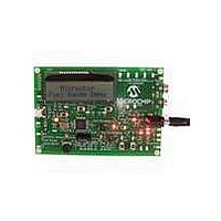
BOARD DEMO FOR MCP3421
Manufacturer
Microchip Technology
Datasheets
1.MCP3421A2T-ECH.pdf
(42 pages)
2.MCP3421DM-BFG.pdf
(26 pages)
3.MCP3421A0T-ECH.pdf
(30 pages)
Specifications of MCP3421DM-BFG
Main Purpose
Power Management, Battery Gauge
Utilized Ic / Part
MCP3421
Processor To Be Evaluated
MCP3421
Lead Free Status / RoHS Status
Lead free / RoHS Compliant
Secondary Attributes
-
Embedded
-
Primary Attributes
-
Lead Free Status / RoHS Status
Lead free / RoHS Compliant, Lead free / RoHS Compliant


MCP3421
5.4
The device acknowledges the general call address
(0x00 in the first byte). The meaning of the general call
address is always specified in the second byte. Refer
to
general calls.
For more information on the general call, or other I
modes, please refer to the Phillips I
5.4.1
The general call reset occurs if the second byte is
‘00000110’ (06h). At the acknowledgement of this
byte, the device will abort current conversion and
perform an internal reset similar to a Power-On-Reset
(POR). All configuration and data register bits are reset
to default values.
5.4.2
The general call conversion occurs if the second byte
is ‘00001000’ (08h). All devices on the bus initiate a
conversion simultaneously. When the device receives
this command, the configuration will be set to the One-
Shot Conversion mode and a single conversion will be
performed. The PGA and data rate settings are
unchanged with this general call.
FIGURE 5-5:
Format.
DS22003E-page 22
START
S
(General Call Address)
Figure
Note:
0 0 0 0 0 0 0 0 A
General Call
First Byte
5-5. The device supports the following two
GENERAL CALL RESET
GENERAL CALL CONVERSION
The I
“00000000” (00h) in the second byte.
2
C specification does not allow
General Call Address
ACK
X
X X X X X X X
Second Byte
2
C specification.
LSB
ACK
STOP
A
S
2
C
5.5
The I
device must be ‘activated’ to operate in high-speed
mode. This is done by sending a special address byte
of “00001XXX” following the START bit. The “XXX” bits
are unique to the High-Speed (HS) mode Master. This
byte is referred to as the High-Speed (HS) Master
Mode Code (HSMMC). The MCP3421 device does not
acknowledge this byte. However, upon receiving this
code, the device switches on its HS mode filters and
communicates up to 3.4 MHz on SDA and SCL bus
lines. The device will switch out of the HS mode on the
next STOP condition.
For more information on the HS mode, or other I
modes, please refer to the Phillips I
5.6
The I
protocol:
• Data transfer may be initiated only when the bus
• During data transfer, the data line must remain
Accordingly, the following bus conditions have been
defined using
5.6.1
Both data and clock lines remain HIGH.
5.6.2
A HIGH to LOW transition of the SDA line while the
clock (SCL) is HIGH determines a START condition. All
commands must be preceded by a START condition.
5.6.3
A LOW to HIGH transition of the SDA line while the
clock (SCL) is HIGH determines a STOP condition. All
operations can be ended with a STOP condition.
5.6.4
The state of the data line represents valid data when,
after a START condition, the data line is stable for the
duration of the HIGH period of the clock signal.
The data on the line must be changed during the LOW
period of the clock signal. There is one clock pulse per
bit of data.
Each data transfer is initiated with a START condition
and terminated with a STOP condition.
is not busy
stable whenever the clock line is HIGH. Changes
in the data line while the clock line is HIGH will be
interpreted as a START or STOP condition
2
C specification requires that a high-speed mode
2
C specification defines the following bus
High-Speed (HS) Mode
I
2
C Bus Characteristics
BUS NOT BUSY (A)
START DATA TRANSFER (B)
STOP DATA TRANSFER (C)
DATA VALID (D)
Figure
5-6.
© 2009 Microchip Technology Inc.
2
C specification.
2
C
Related parts for MCP3421DM-BFG
Image
Part Number
Description
Manufacturer
Datasheet
Request
R

Part Number:
Description:
18-Bit Analog-to-Digital Converter with I2C Interface and On-Board Reference
Manufacturer:
Microchip Technology
Datasheet:

Part Number:
Description:
Manufacturer:
Microchip Technology Inc.
Datasheet:
Part Number:
Description:
Manufacturer:
Microchip Technology Inc.
Datasheet:
Part Number:
Description:
Manufacturer:
Microchip Technology Inc.
Datasheet:
Part Number:
Description:
Manufacturer:
Microchip Technology Inc.
Datasheet:
Part Number:
Description:
Manufacturer:
Microchip Technology Inc.
Datasheet:
Part Number:
Description:
Manufacturer:
Microchip Technology Inc.
Datasheet:
Part Number:
Description:
Manufacturer:
Microchip Technology Inc.
Datasheet:
Part Number:
Description:
Manufacturer:
Microchip Technology Inc.
Datasheet: