AD5247EVAL Analog Devices Inc, AD5247EVAL Datasheet - Page 3
AD5247EVAL
Manufacturer Part Number
AD5247EVAL
Description
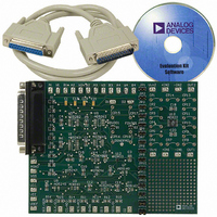
BOARD EVAL FOR AD5247
Manufacturer
Analog Devices Inc
Datasheet
1.AD5247BKSZ50-RL7.pdf
(20 pages)
Specifications of AD5247EVAL
Main Purpose
Digital Potentiometer
Utilized Ic / Part
AD5247
Lead Free Status / RoHS Status
Contains lead / RoHS non-compliant
Secondary Attributes
-
Embedded
-
Primary Attributes
-


SPECIFICATIONS
ELECTRICAL CHARACTERISTICS—5 kΩ VERSION
V
Table 1.
Parameter
DC CHARACTERISTICS—RHEOSTAT MODE
DC CHARACTERISTICS—POTENTIOMETER DIVIDER MODE
RESISTOR TERMINALS
DIGITAL INPUTS AND OUTPUTS
POWER SUPPLIES
DYNAMIC CHARACTERISTICS
1
2
3
4
5
6
7
8
Typical specifications represent average readings at 25°C and V
Resistor position nonlinearity error R-INL is the deviation from an ideal value measured between the maximum resistance and the minimum resistance wiper
positions. R-DNL measures the relative step change from ideal between successive tap positions. Parts are guaranteed monotonic.
V
INL and DNL are measured at V
DNL specification limits of ±1 LSB maximum are guaranteed monotonic under operating conditions.
Resistor Terminal A and Resistor Terminal W have no limitations on polarity with respect to each other.
Guaranteed by design and not subject to production test.
P
All dynamic characteristics use V
DD
A
DISS
Resistor Differential Nonlinearity
Resistor Integral Nonlinearity
Nominal Resistor Tolerance
Resistance Temperature Coefficient
Output Resistance
Differential Nonlinearity
Integral Nonlinearity
Voltage Divider Temperature Coefficient
Full-Scale Error
Zero-Scale Error
Voltage Range
Capacitance A
Capacitance W
Common-Mode Leakage
Input Logic High
Input Logic Low
Input Logic High
Input Logic Low
Input Current
Input Capacitance
Output Logic Low (SDA)
Power Supply Range
Supply Current
Power Dissipation
Power Supply Sensitivity
Bandwidth –3 dB
Total Harmonic Distortion
V
Resistor Noise Voltage Density
= V
W
= 5 V ± 10% or 3 V ± 10%, V
is calculated from (I
Settling Time
DD
, wiper (V
W
) = no connect.
6
5
6
7
6
DD
× V
4
DD
4
W,
). CMOS logic level inputs result in minimum power dissipation.
DD
with the RDAC configured as a potentiometer divider similar to a voltage output DAC. V
6, 8
3
= 5 V.
2
A
2
= V
3
DD
, −40°C < T
A
DD
< +125°C, unless otherwise noted.
= 5 V.
Symbol
R-DNL
R-INL
∆R
∆R
R
DNL
INL
∆V
V
V
V
C
C
I
V
V
V
V
I
C
V
V
I
P
PSSR
BW_5 K
THD
t
e
Rev. E | Page 3 of 20
CM
IL
DD
S
N_WB
WB
WFSE
WZSE
A,
IH
IL
IH
IL
OL
DD RANGE
DISS
A
W
IL
AB
AB
W
V
/∆T
W
/∆T
W
Conditions
R
R
Code = 0x00
Code = 0x40
Code = 0x7F
Code = 0x00
f = 1 MHz, measured to GND,
code = 0x40
f = 1 MHz, measured to GND,
code = 0x40
V
V
V
V
V
V
I
I
V
V
V
code = midscale
R
V
V
R
OL
OL
WB
WB
AB
WB
A
DD
DD
DD
DD
IN
IH
IH
DD
A
A
= V
= 1 V rms, V
= 5 V, ±1 LSB error band
= 3 mA
= 6 mA
= 0 V or 5 V
= 5 V or V
= 5 V or V
, V
, V
= 5 kΩ, code = 0x40
= 5 V
= 5 V
= 3 V
= 3 V
= 5 V ± 10%,
= 2.5 kΩ, R
A
A
DD
= no connect
= no connect
/2
IL
IL
= 0 V
= 0 V, V
B
S
= 0 V, f = 1 kHz
= 0 Ω
DD
= 5 V
A
= V
DD
Min
−1.5
−4
−30
−1
−1
−3
0
GND
2.4
2.1
2.7
and V
B
= 0 V.
Typ
±0.1
±0.75
45
75
±0.1
±0.2
15
−2
1
45
60
1
5
3
±0.003
1.2
0.05
1
6
1
Max
+1.5
+4
+30
300
+1
+1
0
2
V
0.8
0.6
±1
0.4
0.6
5.5
8
40
±0.05
DD
AD5247
Unit
LSB
LSB
%
ppm/°C
Ω
LSB
LSB
ppm/°C
LSB
LSB
V
pF
pF
nA
V
V
V
V
µA
pF
V
V
V
µA
µW
%/%
MHz
%
µs
nV/√Hz
Related parts for AD5247EVAL
Image
Part Number
Description
Manufacturer
Datasheet
Request
R


Part Number:
Description:
±1.7g Dual-Axis IMEMS Accelerometer Evaluation Board
Manufacturer:
Analog Devices Inc
Datasheet:

Part Number:
Description:
Inertial Sensor Evaluation System
Manufacturer:
Analog Devices Inc
Datasheet:
Part Number:
Description:
Manufacturer:
Analog Devices Inc
Datasheet:
Part Number:
Description:
Manufacturer:
Analog Devices Inc
Datasheet:
Part Number:
Description:
Manufacturer:
Analog Devices Inc
Datasheet:
Part Number:
Description:
Manufacturer:
Analog Devices Inc
Datasheet:
Part Number:
Description:
Manufacturer:
Analog Devices Inc
Datasheet:
Part Number:
Description:
Manufacturer:
Analog Devices Inc
Datasheet:
Part Number:
Description:
Manufacturer:
Analog Devices Inc
Datasheet:
Part Number:
Description:
Manufacturer:
Analog Devices Inc
Datasheet:
Part Number:
Description:
Manufacturer:
Analog Devices Inc
Datasheet:
Part Number:
Description:
Manufacturer:
Analog Devices Inc
Datasheet: