LMX25120967EVAL/NOPB National Semiconductor, LMX25120967EVAL/NOPB Datasheet - Page 4
LMX25120967EVAL/NOPB
Manufacturer Part Number
LMX25120967EVAL/NOPB
Description
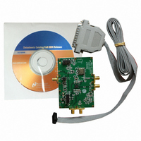
EVALUATION BOARD FOR LMX25120967
Manufacturer
National Semiconductor
Series
PLLatinum™r
Datasheets
1.LMX2512LQ0967NOPB.pdf
(18 pages)
2.LMX2430EVAL.pdf
(8 pages)
3.LMX25120967EVALNOPB.pdf
(24 pages)
Specifications of LMX25120967EVAL/NOPB
Main Purpose
Timing, Frequency Synthesizer
Embedded
No
Utilized Ic / Part
LMX2512
Primary Attributes
Single Fractional-N and Integer-N PLL with VCO
Secondary Attributes
967MHz, CodeLoader Graphical User Interface
Lead Free Status / RoHS Status
Lead free / RoHS Compliant
Other names
*LMX25120967EVAL
*LMX25120967EVAL/NOPB
LMX25120967EVAL
*LMX25120967EVAL/NOPB
LMX25120967EVAL


www.national.com
Symbol
I
I
(I
I
I
REFERENCE OSCILLATOR PARAMETERS
f
V
RF VCO
f
P
L(f)
CC
CC
DD
PD
OSCin
RFout
CC
OSCin
RFout
Absolute Maximum Ratings
2, 3)
If Military/Aerospace specified devices are required,
please contact the National Semiconductor Sales Office/
Distributors for availability and specifications.
Electrical Characteristics
Parameter
Supply Voltage
Voltage on any pin
to GND
Storage Temperature
Range
)
RFout
PARAMETERS
+ I
RF
+
DD
Parameter
Total Supply Current
RF PLL Total Supply Current
Power Down Current (Note 4)
Reference Oscillator Input Frequency
(Note 5)
Reference Oscillator Input Sensitivity
Frequency Range
(Note 6)
RF Output Power
Lock Time
(Note 7)
Reference Spurs
RMS Phase Error
Phase Noise
2nd Harmonic Suppression
3rd Harmonic Suppression
Symbol
V
V
T
STG
CC
I
, V
DD
LMX2502LQ1635
LMX2512LQ0967
LMX2512LQ1065
LMX2502LQ1635
LMX2512LQ0967
LMX2512LQ1065
LMX2502LQ1635
LMX2512LQ0967
LMX2512LQ1065
Ratings
-0.3 to 3.6
-0. 3 to V
-0. 3 to V
-65 to 150
(V
CC
DD
CC
+0.3
+0.3
(Notes 1,
= V
Units
DD
˚C
V
V
V
= 2.8 V, T
Condition
OB_CRL [1:0] = 00
OB_CRL [1:0] = 00
CE = LOW or
RF_EN = 0
IF_EN = 0
19.20 MHz and 19.68
MHz are supported
RF VCO
OB_CRL [1:0] = 11
OB_CRL [1:0] = 10
OB_CRL [1:0] = 01
OB_CRL [1:0] = 00
30 MHz Band for RF
PLL
25 MHz Band for RF
PLL
25 MHz Band for RF
PLL
RF PLL in all band
@
@
@
@
@
@
100 kHz offset
1.25 MHz offset
100 kHz offset
900 kHz offset
100 kHz offset
900 kHz offset
4
A
Recommended Operating
Conditions
Note 1: Absolute Maximum Ratings indicate limits beyond which damage to
the device may occur. Recommended Operating Conditions indicate condi-
tions for which the device is intended to be functional, but do not guarantee
specific performance limits. For guaranteed specifications and test condi-
tions, refer to the Electrical Characteristics section. The guaranteed specifi-
cations apply only for the conditions listed.
Note 2: This device is a high performance RF integrated circuit with an ESD
rating
should be done at ESD protected work stations.
Note 3: GND = 0 V.
Parameter
Ambient Temperature
Supply Voltage (to GND) V
= 25 ˚C; unless otherwise noted)
<
2 kV and is ESD sensitive. Handling and assembly of this device
1619.62
1052.64
954.42
19.20
Min
-2
-5
-7
-9
Symbol
T
A
CC
-113
-138
-117
-139
-117
-139
Typ
500
500
500
0.2
1.3
17
16
, V
-2
-4
-6
1
DD
Min Typ Max Units
-30 25
2.7
1649.62
1077.57
979.35
19.68
-112
-136
-115
-138
-115
-138
Max
V
800
800
800
-75
-25
-20
19
18
20
-1
-3
CC
4
1
85
3.3
degrees
dBc/Hz
dBc/Hz
dBc/Hz
dBc/Hz
dBc/Hz
dBc/Hz
Units
Vp-p
MHz
MHz
MHz
MHz
dBm
dBm
dBm
dBm
dBc
dBc
dBc
mA
mA
µA
µs
µs
µs
˚C
V
Related parts for LMX25120967EVAL/NOPB
Image
Part Number
Description
Manufacturer
Datasheet
Request
R

Part Number:
Description:
National Semiconductor [8-Bit D/A Converter]
Manufacturer:
National Semiconductor
Datasheet:
Part Number:
Description:
National Semiconductor [Media Coprocessor]
Manufacturer:
National Semiconductor
Datasheet:
Part Number:
Description:
Digitally Controlled Tone and Volume Circuit with Stereo Audio Power Amplifier, Microphone Preamp Stage and National 3D Sound
Manufacturer:
National Semiconductor
Datasheet:
Part Number:
Description:
Digitally Controlled Tone and Volume Circuit with Stereo Audio Power Amplifier, Microphone Preamp Stage and National 3D Sound
Manufacturer:
National Semiconductor
Datasheet:
Part Number:
Description:
AC97 Rev 2 Codec with Sample Rate Conversion and National 3D Sound
Manufacturer:
National Semiconductor
Part Number:
Description:
Manufacturer:
National Semiconductor
Datasheet:
Part Number:
Description:
Manufacturer:
National Semiconductor
Datasheet:
Part Number:
Description:
General Purpose, Low Voltage, Low Power, Rail-to-Rail Output Operational Amplifiers
Manufacturer:
National Semiconductor
Datasheet:
Part Number:
Description:
8-bit 20 MSPS flash A/D converter.
Manufacturer:
National Semiconductor
Datasheet:
Part Number:
Description:
Low Noise Quad Operational Amplifier
Manufacturer:
National Semiconductor
Datasheet:
Part Number:
Description:
Quad Differential Line Receivers
Manufacturer:
National Semiconductor
Datasheet:
Part Number:
Description:
Quad High Speed Trapezoidal? Bus Transceiver
Manufacturer:
National Semiconductor
Datasheet:
Part Number:
Description:
Dual Line Receiver
Manufacturer:
National Semiconductor
Datasheet:
Part Number:
Description:
TTL to 10k ECL Level Translator with Latch
Manufacturer:
National Semiconductor
Datasheet: