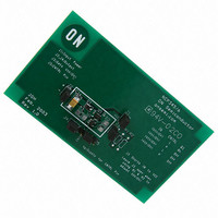
NCP345EVB ON Semiconductor, NCP345EVB Datasheet
NCP345EVB
Manufacturer Part Number
NCP345EVB
Description
EVAL BOARD FOR NCP345
Manufacturer
ON Semiconductor
Specifications of NCP345EVB
Design Resources
NCP345 Demo Board BOM NCP345EVB Gerber Files NCP345/6 EVB Schematic
Main Purpose
Overvoltage Protection
Embedded
No
Utilized Ic / Part
NCP345
Lead Free Status / RoHS Status
Lead free / RoHS Compliant
Secondary Attributes
-
Primary Attributes
-
Lead Free Status / Rohs Status
Lead free / RoHS Compliant
For Use With/related Products
NCP345
Other names
NCP345EVBOS
h
Test Procedure for the NCP345/6 Evaluation Board
8/27/03
Figure 1: NCP345/6 Demo Board Assembly Drawing
Refer to Table 1 for bolded test values in the following procedure.
Table 1: Test Values
V1
V2*
V3
V4**
V5
* This is the power supply voltage minus the voltage drops across Q1 and D1. It might measure slightly
lower than V1.
** Since C1 is a large capacitor a load (specified in step (3) is required for the voltage to decay to 0V in a
timely manner for functional testing.
1) Connect jumper to J3.
2) Connect jumpers between CNTRL and – pins on J5.
3) Connect 50 Ohms to J2 if D3 is unpopulated, otherwise connect to J4.
4) Apply V1 to J1 + and – pins.
5) Measure voltage at J2 if D3 is unpopulated, otherwise connect to J4. It should equal V2.
6) Apply V3 to J1 + and – pins.
7) Wait 1 second.
8) Measure voltage at J2 if D3 is unpopulated, otherwise connect to J4. It should equal V4.
9) Apply V1 to J1 + and – pins.
10) Apply V5 between Vp on J5 and any open - pin on the board.
11) Connect jumper from step (2) between the CNTRL and + pins on J5.
12) Measure voltage at J2 if D3 is unpopulated, otherwise connect to J4. It should equal V4.
NCP345SNT1
6
6
8
0
2
NCP346SN1T1
4
4
5
0
2
NCP346SN2T1
5
5
6
0
2
Unit
V
V
V
V
V
Related parts for NCP345EVB
Image
Part Number
Description
Manufacturer
Datasheet
Request
R

Part Number:
Description:
ON Semiconductor [VOLTAGE REGULATOR]
Manufacturer:
ON Semiconductor
Datasheet:
Part Number:
Description:
357-036-542-201 CARDEDGE 36POS DL .156 BLK LOPRO
Manufacturer:
ON Semiconductor
Datasheet:
Part Number:
Description:
357-036-542-201 CARDEDGE 36POS DL .156 BLK LOPRO
Manufacturer:
ON Semiconductor
Datasheet:
Part Number:
Description:
357-036-542-201 CARDEDGE 36POS DL .156 BLK LOPRO
Manufacturer:
ON Semiconductor
Datasheet:
Part Number:
Description:
357-036-542-201 CARDEDGE 36POS DL .156 BLK LOPRO
Manufacturer:
ON Semiconductor
Datasheet:
Part Number:
Description:
357-036-542-201 CARDEDGE 36POS DL .156 BLK LOPRO
Manufacturer:
ON Semiconductor
Datasheet:
Part Number:
Description:
357-036-542-201 CARDEDGE 36POS DL .156 BLK LOPRO
Manufacturer:
ON Semiconductor
Datasheet:
Part Number:
Description:
357-036-542-201 CARDEDGE 36POS DL .156 BLK LOPRO
Manufacturer:
ON Semiconductor
Datasheet:
Part Number:
Description:
357-036-542-201 CARDEDGE 36POS DL .156 BLK LOPRO
Manufacturer:
ON Semiconductor
Datasheet:
Part Number:
Description:
357-036-542-201 CARDEDGE 36POS DL .156 BLK LOPRO
Manufacturer:
ON Semiconductor
Datasheet:
Part Number:
Description:
357-036-542-201 CARDEDGE 36POS DL .156 BLK LOPRO
Manufacturer:
ON Semiconductor
Datasheet:
Part Number:
Description:
Manufacturer:
ON Semiconductor
Datasheet:
Part Number:
Description:
Manufacturer:
ON Semiconductor
Datasheet: