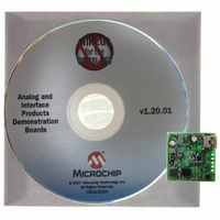
MCP355XDM-TAS Microchip Technology, MCP355XDM-TAS Datasheet - Page 13

MCP355XDM-TAS
Manufacturer Part Number
MCP355XDM-TAS
Description
BOARD DEMO TINY APP SNSR MCP355X
Manufacturer
Microchip Technology
Datasheets
1.MCP3553-ESN.pdf
(36 pages)
2.MCP355XDM-TAS.pdf
(20 pages)
3.MCP355XDM-TAS.pdf
(24 pages)
Specifications of MCP355XDM-TAS
Number Of Adc's
1
Number Of Bits
22
Data Interface
Serial
Inputs Per Adc
1 Single Ended
Input Range
±3 V
Voltage Supply Source
Single Supply
Operating Temperature
-40°C ~ 125°C
Utilized Ic / Part
MCP355x
Processor To Be Evaluated
MCP355x
Interface Type
USB
Silicon Manufacturer
Microchip
Silicon Core Number
MCP3551, MCP3553, MCP3550-50, MCP3550-60
Kit Application Type
Data Converter
Application Sub Type
ADC
Kit Contents
Board Cable Docs
Rohs Compliant
Yes
Lead Free Status / RoHS Status
Not applicable / Not applicable
Lead Free Status / RoHS Status
Lead free / RoHS Compliant, Not applicable / Not applicable
Available stocks
Company
Part Number
Manufacturer
Quantity
Price
Company:
Part Number:
MCP355XDM-TAS
Manufacturer:
MICROCHIP
Quantity:
12 000
© 2006 Microchip Technology Inc.
2.4.2
The board can be powered directly from the USB cable or self-powered. LEDs, D4 and
D7, indicate how the board is powered.
To power the board via the USB, simply connect the USB cable. D7 will illuminate.
To self-power the board, connect a 5V power supply to the power terminals. D4 will
illuminate.
2.4.3
By default, the analog input is provided by a voltage divider circuit on V
shorted to ground via a 0Ω resistor. These components are initially soldered on the
board for demonstration purposes only and are not required by a typical MCP3551
system. These components should be removed when evaluating a sensor through
JPX.
2.4.4
For demonstration purposes, the voltage on the inputs is fixed via a voltage divider on
V
by the two SMA connectors (J1 and J3) and/or the 4-pin header (J10).
There are several reference designators (Zn) which can be populated, as needed, to
evaluate the MCP3551, external circuits, Z1, Z2 and Z3, are populated to create the
voltage divider. These components will need to be removed to accommodate the
custom circuit. All other Zn designators are unpopulated.
2.4.5
The DataView software displays the digital output of the MCP3551 in a graphical format
on Windows
PC through the USB port, where it is converted to decimal and then plotted. The sample
size of each window calculation (Histogram, Output and Auxiliary) can be configured
through the Configuration dialog box. There are three different windows that display the
data.
2.4.5.1
The Output window (Figure 2-2) shows the ADC output as a scope plot. The Y-axis can
be configured LSB (default), PPM, percentage or volts (see Figure 2-5).
2.4.5.2
The Histogram window (Figure 2-3) shows the distribution over the selected sample
size. Each bin of the histogram is always the equivalent of 1 LSB, showing the true
output noise performance of the system with this quanta.
2.4.5.3
The Auxiliary Data window (Figure 2-4) displays calculated information, such as mean
LSB, mean PPM, sample size and output noise RMS (PPM).
2.4.5.4
The Configuration window has three tabs for configuration and information.
The Scope Plot tab allows the Y-axis and the units to be changed. The X-axis is fixed.
The defualt for the Y-axis is ‘Auto’ for the min/max and LSB for the units.
The A/D Device tab displays the ADC used (MCP3551) and is also where the sample
rate for displaying the data is set. Please note that the minimum should be ~90 ms
(see Section 2.4.6 “MCP3551 Sample Rate Demo” for more information).
The USB Device tab displays information about the board/device.
IN
+. However, experimentation with different voltages on the inputs is made possible
Hardware Power
The Analog Input
Customizing the Analog Input
Reading the MCP3551 Output Using the DataView Software
OUTPUT WINDOW
HISTOGRAM WINDOW
AUXILIARY DATA SCREEN
CONFIGURATION WINDOW
®
2000 and Windows XP
®
systems. The 22-bit value is transferred to the
DS51579C-page 9
IN
+, with V
IN
-


