SSM2311-EVALZ Analog Devices Inc, SSM2311-EVALZ Datasheet - Page 15
SSM2311-EVALZ
Manufacturer Part Number
SSM2311-EVALZ
Description
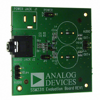
BOARD EVALUATION FOR SSM2311
Manufacturer
Analog Devices Inc
Datasheet
1.SSM2311CBZ-REEL7.pdf
(20 pages)
Specifications of SSM2311-EVALZ
Amplifier Type
Class D
Output Type
1-Channel (Mono)
Max Output Power X Channels @ Load
3.3W x 1 @ 3 Ohm
Voltage - Supply
2.5 V ~ 5.5 V
Operating Temperature
-40°C ~ 85°C
Board Type
Fully Populated
Utilized Ic / Part
SSM2311
Silicon Manufacturer
Analog Devices
Application Sub Type
Audio Power Amplifier - Class D
Kit Application Type
Amplifier
Silicon Core Number
SSM2311
Kit Contents
Board
Lead Free Status / RoHS Status
Lead free / RoHS Compliant
Lead Free Status / RoHS Status
Lead free / RoHS Compliant, Lead free / RoHS Compliant


APPLICATION NOTES
OVERVIEW
The SSM2311 mono Class-D audio amplifier features a filterless
modulation scheme that greatly reduces the external components
count, conserving board space and thus reducing the system’s cost.
The SSM2311 does not require an output filter, but instead relies
on the inherent inductance of the speaker coil and the natural
filtering of the speaker and the human ear to fully recover the audio
component of the square-wave output. While many Class-D ampli-
fiers use some variation of pulse-width modulation (PWM), the
SSM2311 uses Σ-Δ modulation to determine the switching
pattern of the output devices. This provides a number of important
benefits. Σ-Δ modulators do not produce a sharp peak with
many harmonics in the AM frequency band, as pulse-width
modulators often do. Σ-Δ modulation provides the benefits of
reducing the amplitude of spectral components at high frequencies;
that is, reducing EMI emission that might otherwise be radiated
by speakers and long cable traces. Due to the inherent spread-
spectrum nature of Σ-Δ modulation, the need for oscillator
synchronization is eliminated for designs incorporating
multiple SSM2311 amplifiers.
The SSM2311 also offers protection circuits for overcurrent and
temperature protection.
GAIN
The SSM2311 has a default gain of 18 dB, but can be reduced by
using a pair of external resistors with a value calculated as follows:
POP-AND-CLICK SUPPRESSION
Voltage transients at the output of audio amplifiers can occur when
shutdown is activated or deactivated. Voltage transients as low
as 10 mV can be heard as an audio pop in the speaker. Clicks
and pops can also be classified as undesirable audible transients
generated by the amplifier system and therefore as not coming
from the system input signal. Such transients can be generated
when the amplifier system changes its operating mode. For example,
the following can be sources of audible transients: system power-up/
power-down, mute/unmute, input source change, and sample rate
change. The SSM2311 has a pop-and-click suppression architecture
that reduces these output transients, resulting in noiseless activation
and deactivation.
LAYOUT
As output power continues to increase, care needs to be taken to
lay out PCB traces and wires properly between the amplifier,
load, and power supply. A good practice is to use short, wide
PCB tracks to decrease voltage drops and minimize inductance.
Ensure that track widths are at least 200 mil for every inch of
External Gain Settings = 300k/(37.5k + Rext)
Rev. 0 | Page 15 of 20
track length for lowest DCR, and use 1 oz or 2 oz of copper PCB
traces to further reduce IR drops and inductance. A poor layout
increases voltage drops, consequently affecting efficiency. Use
large traces for the power supply inputs and amplifier outputs to
minimize losses due to parasitic trace resistance.
Proper grounding guidelines help to improve audio
performance, minimize crosstalk between channels, and
prevent switching noise from coupling into the audio signal. To
maintain high output swing and high peak output power, the
PCB traces that connect the output pins to the load and supply
pins should be as wide as possible to maintain the minimum
trace resistances. It is also recommended to use a large-area
ground plane for minimum impedances.
In addition, good PCB layouts isolate critical analog paths from
sources of high interference. High frequency circuits (analog
and digital) should be separated from low frequency ones.
Properly designed multilayer printed circuit boards can reduce
EMI emission and increase immunity to the RF field by a factor of
10 or more compared with double-sided boards. A multilayer
board allows a complete layer to be used for the ground plane,
whereas the ground plane side of a double-sided board is often
disrupted with signal crossover. If the system has separate analog
and digital ground and power planes, the analog ground plane
should be underneath the analog power plane, and, similarly, the
digital ground plane should be underneath the digital power
plane. There should be no overlap between analog and digital
ground planes or analog and digital power planes.
–10
70
60
50
40
30
20
10
0
30
Figure 47. EMI Emissions from SSM2311
100
FREQUENCY (MHz)
SSM2311
1000
Related parts for SSM2311-EVALZ
Image
Part Number
Description
Manufacturer
Datasheet
Request
R

Part Number:
Description:
SSM2311 EVALUATION BOARD-Mini 7mm X 7mm
Manufacturer:
Analog Devices Inc
Datasheet:

Part Number:
Description:
±1.7g Dual-Axis IMEMS Accelerometer Evaluation Board
Manufacturer:
Analog Devices Inc
Datasheet:
Part Number:
Description:
Inertial Sensor Evaluation System
Manufacturer:
Analog Devices Inc
Datasheet:
Part Number:
Description:
Manufacturer:
Analog Devices Inc
Datasheet:
Part Number:
Description:
Manufacturer:
Analog Devices Inc
Datasheet:
Part Number:
Description:
Manufacturer:
Analog Devices Inc
Datasheet:
Part Number:
Description:
Manufacturer:
Analog Devices Inc
Datasheet:
Part Number:
Description:
Manufacturer:
Analog Devices Inc
Datasheet:
Part Number:
Description:
Manufacturer:
Analog Devices Inc
Datasheet:
Part Number:
Description:
Manufacturer:
Analog Devices Inc
Datasheet:
Part Number:
Description:
Manufacturer:
Analog Devices Inc
Datasheet:
Part Number:
Description:
Manufacturer:
Analog Devices Inc
Datasheet:
Part Number:
Description:
Manufacturer:
Analog Devices Inc
Datasheet: