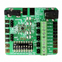
SSM2306-EVALZ Analog Devices Inc, SSM2306-EVALZ Datasheet

SSM2306-EVALZ
Specifications of SSM2306-EVALZ
Related parts for SSM2306-EVALZ
SSM2306-EVALZ Summary of contents
Page 1
... The SSM2306 also has excellent rejection of power supply noise, including noise caused by GSM transmission bursts and RF rectification. The SSM2306 has a preset gain that can be reduced by using external resistors. The SSM2306 is specified over the commercial temperature range (−40°C to +85°C). It has built-in thermal shutdown and output short-circuit protection available in a 16-lead × ...
Page 2
... SSM2306 TABLE OF CONTENTS Features .............................................................................................. 1 Applications....................................................................................... 1 General Description ......................................................................... 1 Functional Block Diagram .............................................................. 1 Revision History ............................................................................... 2 Specifications..................................................................................... 3 Absolute Maximum Ratings............................................................ 4 Thermal Resistance ...................................................................... 4 ESD Caution.................................................................................. 4 Pin Configuration and Function Descriptions............................. 5 Typical Performance Characteristics ............................................. 6 REVISION HISTORY 4/07—Revision 0: Initial Version Typical Application Circuits ......................................................... 11 Application Notes ........................................................................... 12 Overview ..................................................................................... 12 Gain Selection............................................................................. 12 Pop-and-Click Suppression ...
Page 3
... V 0.615 DD = 2 2.5 V 0.275 DD = 5 5 3 3 2 2 5 5.0 V 0. 420 2.0 2 6.5 5.7 5 1.2 0 >100 Ω, A weighting 96 SSM2306 Max Unit − kHz mV 5 kΩ μs kΩ μV dB ...
Page 4
... SSM2306 ABSOLUTE MAXIMUM RATINGS Absolute maximum ratings apply at 25°C, unless otherwise noted. Table 2. Parameter Supply Voltage Input Voltage Common-Mode Input Voltage ESD Susceptibility Storage Temperature Range Operating Temperature Range Junction Temperature Range Lead Temperature (Soldering, 60 sec) Stresses above those listed under Absolute Maximum Ratings may cause permanent damage to the device. This is a stress rating only ...
Page 5
... Inverting Input for Right Channel. Noninverting Input for Right Channel. No Connect. Noninverting Output for Right Channel. Inverting Output for Right Channel. Ground for Output Amplifiers. Power Supply for Output Amplifiers. Power Supply for Output Amplifiers. Ground for Output Amplifiers. Rev Page SSM2306 ...
Page 6
... SSM2306 TYPICAL PERFORMANCE CHARACTERISTICS 100 R = 4Ω, 33µ 18dB 3.6V DD 0.1 0.01 0.001 0.0001 0.001 0.01 0.1 OUTPUT POWER (W) Figure 3. THD + N vs. Output Power into 4 Ω, A 100 R = 8Ω, 33µ 18dB 2. 3.6V DD 0.1 0.01 0.001 0.0001 0.001 0.01 0.1 OUTPUT POWER (W) Figure 4. THD + N vs. Output Power into 8 Ω ...
Page 7
... L NO LOAD 3.0 3.5 4.0 4.5 5.0 SUPPLY VOLTAGE (V) Figure 13. Supply Current vs. Supply Voltage, No Load VDD = 5V VDD = 3.6V VDD = 2.5V 0.1 0.2 0.3 0.4 0.5 0.6 SHUTDOWN VOLTAGE (V) Figure 14. Supply Current vs. Shutdown Voltage SSM2306 0.25W 100k = 5.5 0.7 0.8 ...
Page 8
... SSM2306 3 1kHz A = 18dB 4Ω, 33µH L 2.5 2.0 10% 1.5 1.0 0.5 0 2.5 3.0 3.5 4.0 SUPPLY VOLTAGE (V) Figure 15. Maximum Output Power vs. Supply Voltage 1kHz A = 6dB 4Ω, 33µH L 2.5 2.0 10% 1.5 1.0 0.5 0 2.5 3.0 3.5 4.0 SUPPLY VOLTAGE (V) Figure 16.Maximum Output Power vs. Supply Voltage ...
Page 9
... P (W) O Figure 25. Supply Current vs. Output Power into 8 Ω 4Ω, 33µ FOR BOTH CHANNELS 3. 2. 0.2 0.4 0.6 0.8 1.0 1.2 1.4 1.6 1.8 P (W) O Figure 26. Supply Current vs. Output Power into 4 Ω SSM2306 = 4 Ω 1.4 1 2.0 2.2 ...
Page 10
... SSM2306 0 –10 –20 –30 –40 –50 –60 –70 –80 –90 –100 10 100 1k FREQUENCY (Hz) Figure 27. PSRR vs. Frequency 8Ω, 33µH L –10 –20 –30 –40 –50 –60 –70 –80 10 100 1k FREQUENCY (Hz) Figure 28. CMRR vs. Frequency 3. rms RIPPLE R = 8Ω, 33µH –20 L –40 –60 –80 –100 – ...
Page 11
... Figure 33. Stereo Single-Ended Input Configuration Rev Page VBATT 2.5V TO 5.0V VDD VDD OUTR+ FET OUTR– DRIVER OUTL+ FET OUTL– DRIVER GND GND VBATT 2.5V TO 5.0V VDD VDD OUTR+ FET DRIVER OUTR– OUTL+ FET DRIVER OUTL– GND GND SSM2306 ...
Page 12
... The SSM2306 also offers protection circuits for overcurrent and overtemperature protection. GAIN SELECTION The SSM2306 has a pair of internal resistors that set default gain for the amplifier possible to adjust the SSM2306 gain by using external resistors at the input. To set a gain lower than 18 dB, refer to Figure 32 for the differential input configu- ration and Figure 33 for the single-ended configuration ...
Page 13
... INPUT CAPACITOR SELECTION The SSM2306 does not require input coupling capacitors if the input signal is biased from 1 are required if the input signal is not biased within this recom- mended input dc common-mode voltage range, if high-pass filtering is needed (see Figure 32 using a single-ended source (see Figure 33) ...
Page 14
... MAX 0.90 0.85 0.80 SEATING PLANE ORDERING GUIDE Model Temperature Range SSM2306CPZ-R2 1 −40°C to +85°C 1 SSM2306CPZ-REEL −40°C to +85°C 1 SSM2306CPZ-REEL7 −40°C to +85° RoHS Compliant Part. 3.00 0.60 MAX BSC SQ 0. 2.75 TOP BSC SQ VIEW 9 (BOTTOM VIEW) ...
Page 15
... NOTES Rev Page SSM2306 ...
Page 16
... SSM2306 NOTES ©2007 Analog Devices, Inc. All rights reserved. Trademarks and registered trademarks are the property of their respective owners. D06542-0-4/07(0) Rev Page ...


