DAK-89 Power Integrations, DAK-89 Datasheet - Page 8
DAK-89
Manufacturer Part Number
DAK-89
Description
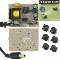
DESIGN ACCELERATOR KIT XT SWITCH
Manufacturer
Power Integrations
Series
LinkSwitch®-XTr
Specifications of DAK-89
Main Purpose
AC/DC, Primary Side
Outputs And Type
1, Isolated
Power - Output
2W
Voltage - Output
6.2V
Current - Output
322mA
Voltage - Input
85 ~ 265VAC
Regulator Topology
Flyback
Board Type
Bare (Unpopulated) and Fully Populated
Utilized Ic / Part
LNK362, LNK363, LNK364
Lead Free Status / RoHS Status
Lead free / RoHS Compliant
Frequency - Switching
-
Lead Free Status / Rohs Status
Lead free / RoHS Compliant
Other names
596-1105


The controller regulates the output voltage by skipping switching cycles (ON/OFF control)
whenever the output voltage is above the reference level. During normal operation,
MOSFET switching is disabled whenever the current flowing into the FEEDBACK (FB)
pin is greater than 49 µA.
oscillator’s (internal) clock signal occurs, MOSFET switching is enabled for that switching
cycle and the MOSFET turns on. That switching cycle terminates when the current
through the MOSFET reaches I
switching cycles will be skipped (disabled) resulting in a high effective switching
frequency. As the load reduces, more switching cycles are skipped, which reduces the
effective switching frequency. At no-load, most switching cycles are skipped, which is
what makes the no-load power consumption of supplies designed around the
LinkSwitch-XT family so low, since switching losses are the dominant loss mechanism at
light loading. Additionally, since the amount of energy per switching cycle is fixed by
I
most of the load range. [NOTE * Termination of a switching cycle by the maximum duty
cycle (DC
line-only design (220/240 VAC) is subject to a brown-out condition, where just slightly
over 50 V (the minimum drain voltage required for normal operation) is available to the
supply, and the current through the MOSFET is not reaching I
because of the low input voltage.]
4.3 Feedback
The output voltage of the supply is determined by the sum of the voltages developed
across VR1, R2 and the (forward bias voltage) LED in optocoupler U2A. As the supply
turns on and the output voltage comes into regulation, U2A will become forward biased,
which will turn on its photo-transistor (U2B) causing > 49 µA to flow into the FB pin, and
the next switching cycle to be skipped. Resistor R2 limits the bias current through VR1 to
about 1 mA. Resistor R3 can be used to fine-tune the output voltage, and also limits the
peak current through U2A during load transients.
feedback each switching cycle (the decision to enable or disable MOSFET switching is
made right before that switching cycle is to occur), the feedback loop requires no
frequency compensation components.
LIMIT
, the skipping of switching cycles gives the supply a fairly consistent efficiency over
MAX
Power Integrations
Tel: +1 408 414 9200 Fax: +1 408 414 9201
www.powerint.com
) signal usually only occurs in an abnormal condition, such as when a high-
If less than 49 µA is flowing into the FB pin when the
LIMIT
, or the DC
MAX
signal occurs*.
Since the controller responds to
LIMIT
each switching cycle
At full load, few
Page 8 of 32
Related parts for DAK-89
Image
Part Number
Description
Manufacturer
Datasheet
Request
R

Part Number:
Description:
KIT DESIGN ACCELERATOR MODEM
Manufacturer:
Power Integrations
Datasheet:

Part Number:
Description:
KIT DESIGN ACCELERATOR SET TOP
Manufacturer:
Power Integrations
Datasheet:

Part Number:
Description:
KIT REF DES DPA 6.6W DC-DC CONV
Manufacturer:
Power Integrations
Datasheet:

Part Number:
Description:
KIT DESIGN ACCELERATOR POE CONV
Manufacturer:
Power Integrations
Datasheet:

Part Number:
Description:
DESIGN ACCELERATOR KIT LP SWITCH
Manufacturer:
Power Integrations
Datasheet:

Part Number:
Description:
KIT DESIGN ACC PEAKSWITCH FAMILY
Manufacturer:
Power Integrations
Datasheet:

Part Number:
Description:
KIT DESIGN ACCELERATOR ADAPTER
Manufacturer:
Power Integrations
Datasheet:

Part Number:
Description:
KIT DESIGN ACCELERATOR ADAPTER
Manufacturer:
Power Integrations
Datasheet:

Part Number:
Description:
KIT DESIGN ACCELERATOR DC-DC
Manufacturer:
Power Integrations
Datasheet:

Part Number:
Description:
KIT DESIGN ACCELERATOR DPA SW
Manufacturer:
Power Integrations
Datasheet: