DAK-89 Power Integrations, DAK-89 Datasheet - Page 2
DAK-89
Manufacturer Part Number
DAK-89
Description
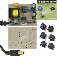
DESIGN ACCELERATOR KIT XT SWITCH
Manufacturer
Power Integrations
Series
LinkSwitch®-XTr
Specifications of DAK-89
Main Purpose
AC/DC, Primary Side
Outputs And Type
1, Isolated
Power - Output
2W
Voltage - Output
6.2V
Current - Output
322mA
Voltage - Input
85 ~ 265VAC
Regulator Topology
Flyback
Board Type
Bare (Unpopulated) and Fully Populated
Utilized Ic / Part
LNK362, LNK363, LNK364
Lead Free Status / RoHS Status
Lead free / RoHS Compliant
Frequency - Switching
-
Lead Free Status / Rohs Status
Lead free / RoHS Compliant
Other names
596-1105


Rev. E 11/08
Figure 2. Functional Block Diagram.
Pin Functional Description
DRAIN (D) Pin:
Power MOSFET drain connection. Provides internal operating
current for both startup and steady-state operation.
BYPASS (BP) Pin:
Connection point for a 0.1 μF external bypass capacitor for the
internally generated 5.8 V supply. If an external bias winding is
used, the current into the BP pin must not exceed 1 mA.
FEEDBACK (FB) Pin:
During normal operation, switching of the power MOSFET is
controlled by this pin. MOSFET switching is disabled when a
current greater than 49 μA is delivered into this pin.
SOURCE (S) Pin:
This pin is the power MOSFET source connection. It is also the
ground reference for the BYPASS and FEEDBACK pins.
2-2
2
2
FEEDBACK
BYPASS
(FB)
(BP)
LNK362-364
V
FB
-V
TH
6.3 V
OSCILLATOR
JITTER
COUNTER
RESTART
CLOCK
AUTO-
DC
CLOCK
RESET
MAX
PRESENT
FAULT
5.8 V
4.8 V
Figure 3. Pin Confi guration.
SHUTDOWN
THERMAL
BP
FB
G Package (SMD-8B)
P Package (DIP-8B)
S
S
+
-
S
R
1
2
3
4
BYPASS PIN
UNDER-VOLTAGE
Q
Q
3a
REGULATOR
5.8 V
8
7
5
S
D
S
CURRENT LIMIT
COMPARATOR
BLANKING
LEADING
EDGE
D Package (SO-8C)
BP
FB
D
+
-
1
2
4
V I
LIMIT
3b
PI-4232-110205
PI-3491-120706
SOURCE
8
7
6
5
DRAIN
(D)
(S)
S
S
S
S
Related parts for DAK-89
Image
Part Number
Description
Manufacturer
Datasheet
Request
R

Part Number:
Description:
KIT DESIGN ACCELERATOR MODEM
Manufacturer:
Power Integrations
Datasheet:

Part Number:
Description:
KIT DESIGN ACCELERATOR SET TOP
Manufacturer:
Power Integrations
Datasheet:

Part Number:
Description:
KIT REF DES DPA 6.6W DC-DC CONV
Manufacturer:
Power Integrations
Datasheet:

Part Number:
Description:
KIT DESIGN ACCELERATOR POE CONV
Manufacturer:
Power Integrations
Datasheet:

Part Number:
Description:
DESIGN ACCELERATOR KIT LP SWITCH
Manufacturer:
Power Integrations
Datasheet:

Part Number:
Description:
KIT DESIGN ACC PEAKSWITCH FAMILY
Manufacturer:
Power Integrations
Datasheet:

Part Number:
Description:
KIT DESIGN ACCELERATOR ADAPTER
Manufacturer:
Power Integrations
Datasheet:

Part Number:
Description:
KIT DESIGN ACCELERATOR ADAPTER
Manufacturer:
Power Integrations
Datasheet:

Part Number:
Description:
KIT DESIGN ACCELERATOR DC-DC
Manufacturer:
Power Integrations
Datasheet:

Part Number:
Description:
KIT DESIGN ACCELERATOR DPA SW
Manufacturer:
Power Integrations
Datasheet: