IRDC3621 International Rectifier, IRDC3621 Datasheet - Page 11
IRDC3621
Manufacturer Part Number
IRDC3621
Description
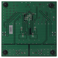
BOARD EVAL DUAL SYNC BUCK CTRLR
Manufacturer
International Rectifier
Datasheet
1.IR3621MTR.pdf
(29 pages)
Specifications of IRDC3621
Main Purpose
DC/DC, Step Down
Outputs And Type
2, Non-Isolated
Voltage - Output
1.8V, 2.5V
Current - Output
10A, 10A
Voltage - Input
5.5 ~ 14.5V
Regulator Topology
Buck
Frequency - Switching
400kHz
Board Type
Fully Populated
Utilized Ic / Part
IR3621
Lead Free Status / RoHS Status
Lead free / RoHS Compliant
Power - Output
-


APPLICATION INFORMATION
Design Example:
The following example is a typical application for the
IR3621, the schematic is Figure19 on page18.
Output Voltage Programming
Output voltage is programmed by the reference voltage
and an external voltage divider. The Fb1 pin is the invert-
ing input of the error amplifier, which is referenced to the
voltage on the non-inverting pin of error amplifier. For this
application, this pin (V
voltage (V
following equation:
When an external resistor divider is connected to the
output as shown in Figure 11.
Equation (4) can be rewritten as:
If the high value feedback resistors are used, the input
bias current of the Fb pin could cause a slight increase
in output voltage. The output voltage can be set more
accurately by using low value, precision resistors.
Figure 11 - Typical application of the IR3621 for pro-
Will result to:
V
V
V
R
V
V
V
V
∆V
F
OUT
P2
OUT(2.5V)
REF
9
S
IN
OUT(2.5V)
OUT(1.8V)
= 2.15K, R
= 400kHz
OUT
= V
= 12V
R
= 0.8V
= V
REF
6
= Output voltage ripple 3% of V
REF
= R
). The output voltage is defined by using the
gramming the output voltage.
P2
= 2.5V
= 2.5V @ 10A
= 1.8V @ 10A
V
V
= 0.8V
× 1 +
REF
P2
5
IR3621
(
×
5
= 1K
(
V
P2
R
R
V
OUT
) is connected to the reference
6
5
P
)
Fb
- 1
)
V
V
R
OUT(1.8V)
REF
7
= 1.24K, R
---(4)
= 0.8
= 1.8V
V
OUT
R
R
8
OUT
6
5
= 1K
www.irf.com
Soft-Start Programming
The soft-start timing can be programmed by selecting
the soft-start capacitance value. The start-up time of
the converter can be calculated by using:
For a start-up time of 4ms for both output, the soft-start
capacitor will be 0.1µF. Connect two 0.1 Fceramic
capacitors from SS1 pin and SS2 pin to GND.
Supply VcH1 and VcH2
To drive the high side MOSFET, it is necessary to sup-
ply a gate voltage at least 4V greater than the bus volt-
age. This is achieved by using a charge pump configu-
ration as shown in Figure 12. This method is simple
and inexpensive. The operation of the circuit is as fol-
lows: when the lower MOSFET is turned on, the ca-
pacitor (C1) charges up to V
(D1). The bus voltage will be added to this voltage when
upper MOSFET turns on in next cycle, and providing
supply voltage (VcH1) through diode (D2). VcH1 is ap-
proximately:
Capacitor in the range of 0.1µF is generally adequate
for most applications. The diode must be a fast recov-
ery device to minimize the amount of charge fed back
from the charge pump capacitor into V
need to be able to block the full power rail voltage, which
is seen when the high side MOSFET is switched on.
For low voltage application, Schottky diodes can be
used to minimize forward drop across the diodes at
start up.
Css
Where
IR3621
VCH1
Regulator
28×
t
START
Figure 12 - Charge pump circuit.
V
V
OUT3
t
START
OUT3
is the desired start-up time (ms)
+ V
VcH1
(µF)
BUS
C3
HDrv
- (V
IR3621 & (PbF)
C2
D1
---(5)
OUT3
+ V
D2
D1
, through the diode
D2
C1
)
OUT3
V
. The diodes
BUS
Q2
Q1
L2
11
Related parts for IRDC3621
Image
Part Number
Description
Manufacturer
Datasheet
Request
R

Part Number:
Description:
SCHOTTKY RECTIFIER
Manufacturer:
International Rectifier Corp.
Datasheet:
Part Number:
Description:
SCHOTTKY RECTIFIER
Manufacturer:
International Rectifier Corp.
Datasheet:
Part Number:
Description:
SCHOTTKY RECTIFIER
Manufacturer:
International Rectifier Corp.
Datasheet:
Part Number:
Description:
SCHOTTKY RECTIFIER
Manufacturer:
International Rectifier Corp.
Datasheet:
Part Number:
Description:
SCHOTTKY RECTIFIER
Manufacturer:
International Rectifier Corp.
Datasheet:
Part Number:
Description:
SCHOTTKY RECTIFIER
Manufacturer:
International Rectifier Corp.
Datasheet:
Part Number:
Description:
SCHOTTKY RECTIFIER
Manufacturer:
International Rectifier Corp.
Datasheet:
Part Number:
Description:
SCHOTTKY RECTIFIER
Manufacturer:
International Rectifier Corp.
Datasheet:
Part Number:
Description:
SCHOTTKY RECTIFIER
Manufacturer:
International Rectifier Corp.
Datasheet:
Part Number:
Description:
SCHOTTKY RECTIFIER
Manufacturer:
International Rectifier Corp.
Datasheet:
Part Number:
Description:
SCHOTTKY RECTIFIER
Manufacturer:
International Rectifier Corp.
Datasheet:
Part Number:
Description:
SCHOTTKY RECTIFIER
Manufacturer:
International Rectifier Corp.
Datasheet:
Part Number:
Description:
SCHOTTKY RECTIFIER
Manufacturer:
International Rectifier Corp.
Datasheet:
Part Number:
Description:
SCHOTTKY RECTIFIER
Manufacturer:
International Rectifier Corp.
Datasheet:
Part Number:
Description:
SCHOTTKY RECTIFIER
Manufacturer:
International Rectifier Corp.
Datasheet: