LM5020EVAL National Semiconductor, LM5020EVAL Datasheet

EVALUATION BOARD FOR LM5020

LM5020EVAL

Manufacturer Part Number
LM5020EVAL
Description
EVALUATION BOARD FOR LM5020
Manufacturer
National Semiconductor
Series
PowerWise®r
Datasheets

Specifications of LM5020EVAL

Main Purpose
DC/DC, Step Down
Outputs And Type
1, Isolated
Voltage - Output
3.3V
Current - Output
4.5A
Voltage - Input
30 ~ 75V
Regulator Topology
Buck
Board Type
Fully Populated
Utilized Ic / Part
LM5020
Lead Free Status / RoHS Status
Contains lead / RoHS non-compliant
Power - Output
-
Frequency - Switching
-
Other names
*LM5020EVAL
© 2005 National Semiconductor Corporation
LM5020 Evaluation Board
Introduction
The LM5020 evaluation board is designed to provide the
design engineer with a fully functional non-isolated flyback
power converter to evaluate the LM5020 controller.
The performance of the evaluation board is as follows:
• Input range: 30V to 75V (100V peak)
• Output voltage: 3.3V
• Output current: 0.2 to 4.5A
• Measured efficiency: 85% at 1.5A, 83% at 4.5A
• Board size: 1.25 x 2.5 x 0.5 inches
• Load Regulation: 1.5%
• Line Regulation: 0.1%
• Line UVLO, Current Limit
The printed circuit board consists of 2 layers of 2 ounce
copper on FR4 material with a total thickness of 0.050
inches. Soldermask has been omitted from some areas to
facilitate cooling. The unit is designed for continuous opera-
tion at rated load at
Theory of Operation
The flyback converter is an inductive based converter in
which inductive energy is stored by applying a voltage
across an inductor in a similar manner to that of a boost
converter. Here the similarity ends. A second coupled wind-
ing of the inductor transfers the energy to a secondary side
<
40˚C with normal convection cooling.
AN200953
National Semiconductor
Application Note 1314
Grant Smith
February 2005
rectifier after the voltage has been removed from the first
winding. This allows the converter input and output grounds
to be configured either isolated or non-isolated. There is also
a voltage/current ratio change possible by altering the wind-
ing ratio between the first winding and the second winding. A
semi-regulated auxiliary winding can also be provided.
The flyback transformer is actually a coupled inductor with
multiple windings wound on a single core. For simplification,
we will refer to the first, driven winding, as the primary and
the main output winding as the secondary winding of the
flyback transformer.
The transformer’s primary inductance is typically made as
large as is practical. However, the airgap necessary to store
the cycle energy lowers the obtainable inductance. The
higher the primary inductance, the less input ripple current
will be generated and the less input filtering will be required.
As shown, the LM5020 directly drives a mosfet switch to
apply voltage across the primary. When the switch turns off,
the secondary applies a forward current to the output rectifier
and charges the output capacitor. In applications where the
input voltage is considerably higher than the output voltage,
the turns ratio between primary and secondary will reflect the
input/output voltage ratio and the duty cycle.
The LM5020 is a full-featured controller providing an internal
start-up regulator, soft start, over-current and under-voltage
lockout.
20095301
www.national.com

Related parts for LM5020EVAL

LM5020EVAL Summary of contents

Page 1

... Here the similarity ends. A second coupled wind- ing of the inductor transfers the energy to a secondary side © 2005 National Semiconductor Corporation National Semiconductor Application Note 1314 Grant Smith ...

Page 2

Powering and Loading Considerations When applying power to the LM5020 evaluation board cer- tain precautions should be followed. The LM5020 evaluation board is quite forgiving of load and input power variations. The possibility of shipping damage or infant failure is ...

Page 3

Performance Characteristics TURN-ON WAVEFORMS When applying power to the LM5020 evaluation board a certain sequence of events must occur. The soft-start feature allows for a minimal output voltage for a short time until the feedback loop can stabilize without overshoot. ...

Page 4

Performance Characteristics (Continued) Trace 1: Input Voltage, at 30VDC. Volts/div = 20.0V Trace 2: Output Voltage, at full load. Volts/div = 2.0V Trace 3: Output Current, at full load. Amps/div = 2.0A Horizontal Resolution = 1.0ms/div FIGURE 3. Trace 1: ...

Page 5

Performance Characteristics (Continued) TRANSFORMER WAVEFORMS Figure 7, Figure 8 and Figure 9 show typical waveforms at the junction of Q1 mosfet and the transformer primary wind- ing. Also shown are typical waveforms at the junction of the transformer secondary and ...

Page 6

www.national.com 6 ...

Page 7

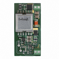
Layout and Bill of Materials The Bill of Materials is shown below and includes the manu- facturer and part number. The layers of the printed circuit board are shown in top down order. View is from the top Designator Description ...

Page 8

PCB Layouts www.national.com 8 20095313 20095314 ...

Page 9

PCB Layouts (Continued) 9 20095315 20095316 www.national.com ...

Page 10

... BANNED SUBSTANCE COMPLIANCE National Semiconductor manufactures products and uses packing materials that meet the provisions of the Customer Products Stewardship Specification (CSP-9-111C2) and the Banned Substances and Materials of Interest Specification (CSP-9-111S2) and contain no ‘‘Banned Substances’’ as defined in CSP-9-111S2. ...

Related keywords