SI3460-EVB Silicon Laboratories Inc, SI3460-EVB Datasheet - Page 14
SI3460-EVB
Manufacturer Part Number
SI3460-EVB
Description
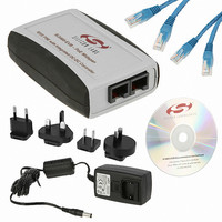
BOARD EVAL POE FOR SI3460
Manufacturer
Silicon Laboratories Inc
Type
DC/DC Switching Converters, Regulators & Controllersr
Specifications of SI3460-EVB
Main Purpose
Special Purpose DC/DC, Power Over Ethernet
Outputs And Type
1, Non-Isolated
Voltage - Output
-48V
Board Type
Fully Populated
Utilized Ic / Part
Si3460
Input Voltage
12 V, 15 V
Output Voltage
- 48 V
Interface Type
Ethernet
Maximum Operating Temperature
+ 85 C
Minimum Operating Temperature
- 40 C
Product
Power Management Modules
For Use With/related Products
Si3460
Lead Free Status / RoHS Status
Lead free / RoHS Compliant
Current - Output
-
Voltage - Input
-
Power - Output
-
Frequency - Switching
-
Regulator Topology
-
Lead Free Status / Rohs Status
Lead free / RoHS Compliant
Other names
336-1842


Si3460
5. Design Considerations
5.1. Isolation
The Si3460-EVB's PSE output power at V
output power requires that the input be isolated from earth ground. Typically, an ac to dc power supply or "wall
wart" is used to provide the 12 V power so the output of this supply is isolated from earth ground.
5.2. External Component Selection
Detailed notes on external component selection are provided in the Si3460-EVB User's Guide schematics and
BOM. In general, these recommendations must be followed closely to ensure output power stability and ripple
(power stage components), surge protection (surge protection diode), and overall IEEE 802.3 compliance.
5.3. Input DC Supply
The input power supply should be rated for at least 25% higher power level than the output power level chosen.
This is primarily to account for the 75 to 80% nominal efficiency performance of the Si3460-EVB reference design.
For example, to support a Class 0 PSE, for example, the input supply should be capable of supplying 19.25 W
(15.4 W x 1.25 = 19.25 W).
5.4. STATUS and RESET Interface
To reference the RESET and STATUS pins to system ground, the level shifting method shown in Figure 3 can be
used. Refer to the schematic in the Si3460-EVB document.
14
Figure 3. STATUS and RESET Pin Interface when Referenced to System Ground
(66.5 k
(40.2 k
+8.7V
+12V
R8
R7
System Gnd
)
)
OUT
RST CONTROL
U1
is not isolated from the input power source (V
Regulator
TLV431
Shunt
806
(1 k
R22
Rev. 1.1
)
1 uF/
6.3 V
RST
STATUS
VDD
Si3460
Output
Status
(332
R*3.3/2.7
405
R40
)
IN
). Isolation of PSE
Related parts for SI3460-EVB
Image
Part Number
Description
Manufacturer
Datasheet
Request
R

Part Number:
Description:
IC POWER MANAGEMENT CTLR 11VQFN
Manufacturer:
Silicon Laboratories Inc
Datasheet:

Part Number:
Description:
IC POWER MANAGEMENT CTLR 11VQFN
Manufacturer:
Silicon Laboratories Inc
Datasheet:
Part Number:
Description:
IC POWER MANAGEMENT CTLR 11VQFN
Manufacturer:
Silicon Laboratories Inc
Datasheet:
Part Number:
Description:
IC POWER MANAGEMENT CTLR 11VQFN
Manufacturer:
Silicon Laboratories Inc
Datasheet:

Part Number:
Description:
Hot Swap & Power Distribution IEEE 802.3af PSE w/DC-DC CTRLR
Manufacturer:
Silicon Laboratories Inc
Datasheet:
Part Number:
Description:
SMD/C°/SINGLE-ENDED OUTPUT SILICON OSCILLATOR
Manufacturer:
Silicon Laboratories Inc
Part Number:
Description:
Manufacturer:
Silicon Laboratories Inc
Datasheet:
Part Number:
Description:
N/A N/A/SI4010 AES KEYFOB DEMO WITH LCD RX
Manufacturer:
Silicon Laboratories Inc
Datasheet:
Part Number:
Description:
N/A N/A/SI4010 SIMPLIFIED KEY FOB DEMO WITH LED RX
Manufacturer:
Silicon Laboratories Inc
Datasheet:
Part Number:
Description:
N/A/-40 TO 85 OC/EZLINK MODULE; F930/4432 HIGH BAND (REV E/B1)
Manufacturer:
Silicon Laboratories Inc
Part Number:
Description:
EZLink Module; F930/4432 Low Band (rev e/B1)
Manufacturer:
Silicon Laboratories Inc
Part Number:
Description:
I°/4460 10 DBM RADIO TEST CARD 434 MHZ
Manufacturer:
Silicon Laboratories Inc
Part Number:
Description:
I°/4461 14 DBM RADIO TEST CARD 868 MHZ
Manufacturer:
Silicon Laboratories Inc
Part Number:
Description:
I°/4463 20 DBM RFSWITCH RADIO TEST CARD 460 MHZ
Manufacturer:
Silicon Laboratories Inc