MCP1650DM-DDSC1 Microchip Technology, MCP1650DM-DDSC1 Datasheet - Page 21
MCP1650DM-DDSC1
Manufacturer Part Number
MCP1650DM-DDSC1
Description
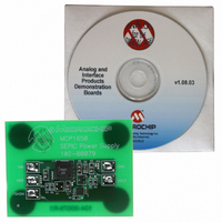
BOARD DEMO FOR MCP1650 SEPIC
Manufacturer
Microchip Technology
Type
DC/DC Switching Converters, Regulators & Controllersr
Specifications of MCP1650DM-DDSC1
Main Purpose
DC/DC, Step Up or Down
Outputs And Type
1, Non-Isolated
Voltage - Output
5V
Current - Output
160mA
Voltage - Input
3 ~ 7V
Regulator Topology
Boost
Frequency - Switching
750kHz
Board Type
Fully Populated
Utilized Ic / Part
MCP1650
Input Voltage
3 V to 7 V
Output Voltage
5 V
Product
Power Management Modules
For Use With/related Products
MCP1650R-E/MS
Lead Free Status / RoHS Status
Contains lead / RoHS non-compliant
Power - Output
-
Lead Free Status / Rohs Status
Lead free / RoHS Compliant


Figure 6-2 represents the top wiring for the MCP1650/
51/52/53 application shown.
As shown in Figure 6-2, the high-current wiring is short
and wide. In this example, a 1 oz. copper layer is used
for both the top and bottom layers. The ground plane
connected to C2 and R4 are connected through the
vias (holes) connecting the top and bottom layer. The
feedback signal (from TP2) is wired from the output of
the regulator around the high current switching section
to the feedback voltage divider and to the FB pin of the
MCP1650/51/52/53.
FIGURE 6-2:
2004 Microchip Technology Inc.
Top Layer Wiring.
Figure 6-3 represents the bottom wiring for the
MCP1650/51/52/53 application shown.
Silk-screen reference designator labels are transparent
from the top of the board. The analog ground plane and
power ground plane are connected near the ground
connection of the input capacitor (C
high-power, ground-circulating currents from flowing
through the analog ground plane.
FIGURE 6-3:
MCP1650/51/52/53
Bottom Layer Wiring.
DS21876A-page 21
2
). This prevents
Related parts for MCP1650DM-DDSC1
Image
Part Number
Description
Manufacturer
Datasheet
Request
R

Part Number:
Description:
BOARD DEMO FOR MCP1650 WHITE LED
Manufacturer:
Microchip Technology
Datasheet:

Part Number:
Description:
BOARD DEMO FOR MCP165X
Manufacturer:
Microchip Technology
Datasheet:

Part Number:
Description:
Manufacturer:
Microchip Technology Inc.
Datasheet:
Part Number:
Description:
Manufacturer:
Microchip Technology Inc.
Datasheet:
Part Number:
Description:
Manufacturer:
Microchip Technology Inc.
Datasheet:
Part Number:
Description:
Manufacturer:
Microchip Technology Inc.
Datasheet:
Part Number:
Description:
Manufacturer:
Microchip Technology Inc.
Datasheet:
Part Number:
Description:
Manufacturer:
Microchip Technology Inc.
Datasheet:
Part Number:
Description:
Manufacturer:
Microchip Technology Inc.
Datasheet:
Part Number:
Description:
Manufacturer:
Microchip Technology Inc.
Datasheet: