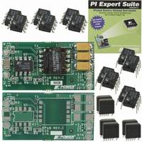
DAK-68A Power Integrations, DAK-68A Datasheet - Page 18
DAK-68A
Manufacturer Part Number
DAK-68A
Description
KIT DESIGN ACCELERATOR POE CONV
Manufacturer
Power Integrations
Series
DPA-Switch®r
Specifications of DAK-68A
Main Purpose
Special Purpose DC/DC, Power Over Ethernet
Outputs And Type
1, Non-Isolated
Power - Output
6.6W
Voltage - Output
3.3V
Current - Output
2A
Voltage - Input
36 ~ 57V
Regulator Topology
Flyback
Frequency - Switching
400kHz
Board Type
Bare (Unpopulated) and Fully Populated
Utilized Ic / Part
DPA423, DPA424, DPA425
Lead Free Status / RoHS Status
Not applicable / Not applicable
Other names
596-1007


Rev. S 12/07
give little or no improvement in effi ciency due to the
improvement in conduction losses being negated by larger
device switching losses. Figure 50 provides information on
switching losses. This together with conduction loss
calculations give an estimate of device dissipation.
Primary Clamp
A primary clamp network is recommended to keep the peak
DRAIN voltage due to primary leakage inductance to below the
BV
capacitor connected across the primary winding is a low cost
and low part count implementation.
Output Rectifi cation
Rectifi cation of the secondary is typically performed using
Schottky diodes or synchronous rectifi cation. Schottky diodes
are selected for peak inverse voltage, output current, forward
drop and thermal conditions. Synchronous rectifi cation
requires the additional complication of providing gate drive. The
specifi ed line under-voltage and line overvoltage thresholds of
DPA-Switch simplifi es deriving gate drive directly from the
transformer secondary winding for many applications. The
turns ratio of the transformer together with the under/
overvoltage thresholds defi nes the minimum and maximum
gate voltages, removing the need for Zeners to clamp the gate
voltage.
Soft-Start
Generally a power supply experiences maximum stress at start-
up before the feedback loop achieves regulation. For a period
of 5 ms the on-chip soft-start linearly increases the duty cycle
from zero to the default DC
primary current limit increases from 85% to 100% over the
same period. This causes the output voltage to rise in an
orderly manner allowing time for the feedback loop to take
control of the duty cycle. This integrated soft-start reduces the
stress on the DPA-Switch MOSFET, clamp circuit and output
diode(s), and helps prevent transformer saturation during start-
up. Also, soft-start limits the amount of output voltage
overshoot, and in many applications eliminates the need for a
soft-fi nish capacitor. If necessary, to remove output overshoot,
a soft-fi nish capacitor may be added to the secondary
reference.
Switching Frequency
The FREQUENCY pin of DPA-Switch offers a switching
frequency option of 400 kHz or 300 kHz. Operating at 300 kHz
will increase the amount of magnetization energy stored in the
transformer. This is ideal for applications using synchronous
rectifi cation driven directly from the transformer secondary
where this energy can be used to drive the catch MOSFET gate.
Transformer Design
It is recommended that the forward converter transformer be
designed for maximum operating fl ux swing of 1500 Gauss and
a peak fl ux density of 3500 Gauss. When operating at the
maximum current limit of the selected DPA-Switch (during
overload conditions), neither magnetic component (transformer
and output inductor) should be allowed to saturate. When a
larger device than necessary has been selected, reducing the
internal current limit close to the operating peak current limits
18
DSS
specifi cation. A Zener diode combined with a small value
DPA422-426
MAX
at turn-on. In addition, the
overload power and minimizes the size of the secondary
components.
No-load and Standby Consumption
Cycle skipping operation at light or no load can signifi cantly
reduce power loss. In addition this operating mode ensures
that the output maintains regulation even without an external
minimum load. However, if cycle skipping is undesirable in a
particular application, it can be avoided by adding suffi cient
pre-load.
DPA-Switch Layout Considerations
The DPA-Switch can operate with large DRAIN current, the
following guidelines should be carefully followed.
Primary Side Connections
The tab of DPA-Switch R package is the intended return path
for the high switching currents. Therefore, the tab should be
connected by wide, low impedance traces back to the input
decoupling capacitor. The SOURCE pin should not be used to
return the power currents; incorrect operation of the device may
result. The SOURCE is only intended as a signal ground. The
device tab (SOURCE) is the correct connection for high current
with the R package.
The CONTROL pin bypass capacitor should be located as
close as possible to the SOURCE and CONTROL pins and its
SOURCE connection trace should not be shared by the main
MOSFET switching currents. All SOURCE pin referenced
components connected to the LINE-SENSE or EXTERNAL
CURRENT LIMIT pins should also be located closely between
their respective pin and SOURCE. Once again, the SOURCE
connection trace of these components should not be shared by
the main MOSFET switching currents. It is critical that the tab
(SOURCE) power switching currents are returned to the input
capacitor through a separate trace that is not shared by the
components connected to CONTROL, LINE-SENSE or
EXTERNAL CURRENT LIMIT pins.
Any traces to the L or X pins should be kept as short as
possible and away from the DRAIN trace to prevent noise
coupling. LINE-SENSE resistor (R1 in Figure 25) should be
located close to the L pin to minimize the trace length on the
L pin side.
In addition to the CONTROL pin capacitor (C6 in Figure 25), a
high frequency bypass capacitor in parallel is recommended as
close as possible between SOURCE and CONTROL pins for
better noise immunity. The feedback optocoupler output
should also be located close to the CONTROL and SOURCE
pins of DPA-Switch.
Heat Sinking
To maximize heat sinking of the DPA-Switch R or G package
and the other power components, special thermally conductive
PC board material (aluminum clad PC board) is recommended.
This has an aluminum sheet bonded to the PC board during the
manufacturing process to provide heat sinking directly and
allow the attachment of an external heat sink. If normal PC
board material is used (such as FR4), providing copper areas on
www.powerint.com
Related parts for DAK-68A
Image
Part Number
Description
Manufacturer
Datasheet
Request
R

Part Number:
Description:
KIT DESIGN ACCELERATOR MODEM
Manufacturer:
Power Integrations
Datasheet:

Part Number:
Description:
KIT DESIGN ACCELERATOR SET TOP
Manufacturer:
Power Integrations
Datasheet:

Part Number:
Description:
KIT REF DES DPA 6.6W DC-DC CONV
Manufacturer:
Power Integrations
Datasheet:

Part Number:
Description:
DESIGN ACCELERATOR KIT XT SWITCH
Manufacturer:
Power Integrations
Datasheet:

Part Number:
Description:
DESIGN ACCELERATOR KIT LP SWITCH
Manufacturer:
Power Integrations
Datasheet:

Part Number:
Description:
KIT DESIGN ACC PEAKSWITCH FAMILY
Manufacturer:
Power Integrations
Datasheet:

Part Number:
Description:
KIT DESIGN ACCELERATOR ADAPTER
Manufacturer:
Power Integrations
Datasheet:

Part Number:
Description:
KIT DESIGN ACCELERATOR ADAPTER
Manufacturer:
Power Integrations
Datasheet:

Part Number:
Description:
KIT DESIGN ACCELERATOR DC-DC
Manufacturer:
Power Integrations
Datasheet:

Part Number:
Description:
KIT DESIGN ACCELERATOR DPA SW
Manufacturer:
Power Integrations
Datasheet: