RDK-83 Power Integrations, RDK-83 Datasheet - Page 9
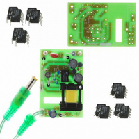
RDK-83
Manufacturer Part Number
RDK-83
Description
KIT DESIGN REF LINKSWITCH LP
Manufacturer
Power Integrations
Series
LinkSwitch®-LPr
Specifications of RDK-83
Main Purpose
AC/DC, Primary Side
Outputs And Type
1, Isolated
Power - Output
1.6W
Voltage - Output
7.7V
Current - Output
210mA
Voltage - Input
85 ~ 265VAC
Regulator Topology
Flyback
Frequency - Switching
66kHz
Board Type
Bare (Unpopulated) and Fully Populated
Utilized Ic / Part
LNK562, LNK563, LNK564
Lead Free Status / RoHS Status
Not applicable / Not applicable
Other names
596-1128


BYPASS Pin
Charge Current
BYPASS Pin
Voltage
BYPASS Pin
Voltage Hysteresis
BYPASS Pin
Supply Current
CIRCUIT PROTECTION
Current Limit
Power Coeffi cient
Leading Edge
Blanking Time
Thermal Shutdown
Temperature
Thermal Shutdown
Hysteresis
OUTPUT
ON-State
Resistance
OFF-State Drain
Leakage Current
Breakdown Voltage
DRAIN Supply
Voltage
Output Enable
Delay
Output Disable
Setup Time
CONTROL FUNCTIONS (cont.)
Parameter
Symbol
R
BV
V
I
T
I
I
I
V
T
I
t
BPSC
t
DS(ON)
LIMIT
t
CH1
CH2
I
LEB
DSS
DST
SHD
BPH
EN
2
SD
BP
DSS
f
di/dt = 40 mA/μs
SOURCE = 0 V; T
V
V
V
BP
BP
BP
T
(Unless Otherwise Specifi ed)
J
= 6.2 V, V
= 0 V, T
= 4 V, T
I
D
= 25 °C
See Note H, T
= 13 mA
V
BP
di/dt = 40 mA/μs
Conditions
See Figure 10
= 6.2 V, V
See Figure 8
See Note G
See Note E
See Note F
J
J
T
T
T
= 25 °C, See Note D
= 25 °C, See Note D
J
J
J
FB
= 25 °C
= 25 °C
= 25 °C
≥2 V, V
J
= -40 to 125 °C
J
FB
= 25 °C
≥2 V,
LNK562
LNK563
LNK564
T
DS
T
J
J
= 100 °C
= 560 V,
= 25 °C
1099
1381
1665
Min
5.55
-5.5
-3.8
124
220
135
700
0.8
84
50
1221
1535
1850
Typ
0.95
-3.3
-2.3
136
265
142
5.8
0.5
75
48
76
LNK562-564
Max
1380
1735
2091
6.10
-1.8
-1.0
148
150
1.2
55
88
50
17
Units
A
mA
mA
μA
μA
ns
°C
°C
μs
μs
2
Ω
V
V
V
V
Rev. H 11/08
Hz
9
Related parts for RDK-83
Image
Part Number
Description
Manufacturer
Datasheet
Request
R

Part Number:
Description:
KIT REF DESIGN 36-72W MOTOR DRVR
Manufacturer:
Power Integrations
Datasheet:

Part Number:
Description:
KIT REF DESIGN FOR LNK457D
Manufacturer:
Power Integrations
Datasheet:

Part Number:
Description:
REFERENCE DESIGN LINKSWITCH-PH
Manufacturer:
Power Integrations
Datasheet:

Part Number:
Description:
Specifications: Manufacturer: Power Integrations ; Output Voltage: 380 VDC ; Input / Supply Voltage (Max): 264 VAC ; Input / Supply Voltage (Min): 90 VAC ; Mounting Style: Through Hole ; Output Current: 0.913 A ; Output Power: 347 W
Manufacturer:
Power Integrations, Inc.

Part Number:
Description:
KIT REF DESIGN TOP HX FOR TOP258
Manufacturer:
Power Integrations
Datasheet:

Part Number:
Description:
Power Management Modules & Development Tools TOPSwitch-JX REF. DESIGN KIT
Manufacturer:
Power Integrations
Datasheet:
Part Number:
Description:
Power Management IC Development Tools REF DESIGN RDR-292 PFF LED STREET LIGHT
Manufacturer:
Power Integrations

Part Number:
Description:
KIT REF DESIGN FOR LNK403EG
Manufacturer:
Power Integrations
Datasheet:

Part Number:
Description:
KIT REF DESIGN FOR LNK406EG
Manufacturer:
Power Integrations
Datasheet:

Part Number:
Description:
KIT REF DESIGN DG CAPZERO
Manufacturer:
Power Integrations
Datasheet:

Part Number:
Description:
KIT REF DESIGN LINKSWITCH-CV
Manufacturer:
Power Integrations
Datasheet:

Part Number:
Description:
KIT REF DESIGN LINKSWITCH 2
Manufacturer:
Power Integrations
Datasheet:

Part Number:
Description:
KIT REF DESIGN PFS762HG
Manufacturer:
Power Integrations
Datasheet:
Part Number:
Description:
Specifications: Family: Eval Boards - DC/DC & AC/DC (Off-Line) SMPS ; Series: HiperLCS™ ; Main Purpose: DC/DC, Step Down ; Outputs and Type: 1, Isolated ; Power - Output: 150W ; Voltage - Output: 24V ; Current - Output: 6.25A ; Voltage - Input:
Manufacturer:
Power Integrations, Inc.
Datasheet:

Part Number:
Description:
KIT REF DESIGN 1.2W PS TN FAMILY
Manufacturer:
Power Integrations
Datasheet: