IRDCIP1203-A International Rectifier, IRDCIP1203-A Datasheet
IRDCIP1203-A
Specifications of IRDCIP1203-A


Related parts for IRDCIP1203-A

IRDCIP1203-A Summary of contents
Page 1
Features • 5.5V to 13.2V Input Voltage • 0. Output Voltage • 15A Maximum Load Capability • 200-400kHz Nominal Switching Frequency • Over Current Hiccup • External Synchronization Capable • Overvoltage Protection • Over Temperature Protection • Internal ...
Page 2
All specifications @ 25°C (unless otherwise specified) Absolute Maximum Ratings Parameter V IN Feedback Output Overvoltage Sense PGOOD Soft Start SYNC Output RMS Current Block Temperature Recommended Operating Conditions Parameter Input Voltage Range Output RMS Current Output Voltage Range ...
Page 3
Electrical Specifications (continued) Parameter Frequency SYNC Frequency Range SYNC Pulse Duration SYNC, High Level Threshold Voltage SYNC, Low Level Threshold Voltage V Quiescent Current IN Thermal Shutdown Max Duty Cycle V Undervoltage Lockout IN Threshold Voltage V Undervoltage Lockout IN ...
Page 4
Internal Block Diagram www.irf.com ...
Page 5
12V V OUT = 1. 300kHz L = 1.0µH T BLK = 125° OUT ...
Page 6
V OUT = 1.5V I OUT = 15A 1. 300kHz L = 1.0µH T BLK = 125°C 1.02 1.00 0.98 0. Input Voltage (V) 1.120 12V ...
Page 7
X www.irf.com ≈ ≈ ≈ ≈ Case Temperature (º 12V IN iP1203 SOA = ...
Page 8
OUT f SW L=1.0uH Vin Average iP1203 FB 8 ≈ Case Temperature (ºC) Unadjusted SOA curve ...
Page 9
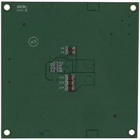
V SWs V SW www.irf.com PGND PGND PGND PGND PGND PGND SYNC OCSET V PGND SW Fig. 11: Recommended PCB Footprint (Top View) V PGND REF T PGOOD ...
Page 10
Css Fig.12: Soft Start/Enable Circuit 0.8Vtyp V Css V OUT Fig. 13: Power Up Threshold Iss iP1203 3V www.irf.com ...
Page 11
www.irf.com ± iP1203 11 ...
Page 12
Vout FB R5 iP1203 FB S C14 (Optional R26 ss R27 I s µ = − RMS out s s µ www.irf.com ...
Page 13
O ∆ ≤ ∆ ≤ 10 > π 2 × × ESR Ω www.irf.com µ µ iP1203 π O µ 13 ...
Page 14
× × ...
Page 15
esr 19 ramp × π 2 × π × ...
Page 16
π × × π × × ...
Page 17
www.irf.com iP1203 17 ...
Page 18
Pin Assignment www.irf.com ...
Page 19
Layout Guidelines www.irf.com iP1203 Suggested Layout iP1203 19 ...
Page 20
Fig. 24: Typical Application Schematic PGND 21 PGND 20 PGND 17 PGND 7 PGND 5 PGND 4 PGND 3 PGND 2 www.irf.com ...
Page 21
T OP VIEW 0.15 [.006 [0.355 ORIENT AT ION CORNER ID 7 15X K 15X R 12X e BOT T OM VIEW www.irf.com S IDE VIEW [0.355] 0.15 [.006 0.000 ...
Page 22
XXXX XXXX iP1203 iP1203 12.0 (.472) NOT OUT LINE CONFORMS T O EIA-481 & EIA-541. iP1203, BGA 22 16.0 (.630) 0438 XXXX iP1203 FEED DIRECTION Fig. 26: Tape & Reel Information 0438 XXXX iP1203 ...
Page 23
The recommended reflow peak temperature is 220°C to 225°C. The total furnance time is approximately 5 minutes with approximately 10 seconds at the peak temperature. Fig.28: Recommended Solder Profile and Stencil Design This product has been designed and qualified for ...