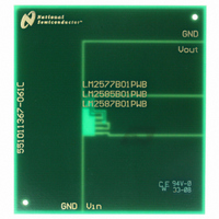
551011367-061 National Semiconductor, 551011367-061 Datasheet - Page 21

551011367-061
Manufacturer Part Number
551011367-061
Description
BOARD WEBENCH LM2577,LM2585/87
Manufacturer
National Semiconductor
Series
WEBENCH® Buildit Boardr
Datasheet
1.LM2577T-15NOPB.pdf
(31 pages)
Specifications of 551011367-061
Main Purpose
DC/DC, Step Up
Regulator Topology
Boost
Board Type
Bare (Unpopulated)
Utilized Ic / Part
LM2577, LM2585, LM2587
Lead Free Status / RoHS Status
Not applicable / Not applicable
Current - Output
-
Voltage - Output
-
Voltage - Input
-
Power - Output
-
Frequency - Switching
-
Outputs And Type
-
Other names
*551011367-061
551011367-061
551011367-061
Application Hints
FLYBACK REGULATOR
A Flyback regulator can produce single or multiple output
voltages that are lower or greater than the input supply
voltage. Figure 18 shows the LM1577/LM2577 used as a
flyback regulator with positive and negative regulated out-
puts. Its operation is similar to a step-up regulator, except the
output switch contols the primary current of a flyback trans-
former. Note that the primary and secondary windings are
out of phase, so no current flows through secondary when
current flows through the primary. This allows the primary to
charge up the transformer core when the switch is on. When
the switch turns off, the core discharges by sending current
through the secondary, and this produces voltage at the
outputs. The output voltages are controlled by adjusting the
peak primary current, as described in the step-up regulator
section.
Voltage and current waveforms for this circuit are shown in
Figure 17, and formulas for calculating them are given in
Figure 19.
FLYBACK REGULATOR DESIGN PROCEDURE
1. Transformer Selection
A family of standardized flyback transformers is available for
creating flyback regulators that produce dual output volt-
ages, from
20lists these transformers with the input voltage, output
voltages and maximum load current they are designed for.
2. Compensation Network (C
Output Capacitor (C
As explained in the Step-Up Regulator Design Procedure,
C
procedure is for a dual output flyback regulator with equal
turns ratios for each secondary (i.e., both output voltages
have the same magnitude). The equations can be used for a
single output regulator by changing
in the following equations.
C
, R
C
and C
±
OUT
10V to
must be selected as a group. The following
±
OUT
15V, as shown in Figure 18. Figure
) Selection
C
(Continued)
, R
C
∑
) and
I
LOAD(max)
to I
LOAD(max)
21
A. First, calculate the maximum value for R
Where
tude) required from both outputs. Select a resistor less than
or equal to this value, and no greater than 3 kΩ.
B. Calculate the minimum value for
at both outputs) using the following two equations.
The larger of these two values must be used to ensure
regulator stability.
FIGURE 17. Flyback Regulator Waveforms
∑
I
LOAD(max)
is the sum of the load current (magni-
∑
C
OUT
01146817
(sum of C
C
.
www.national.com
OUT


