LM20134EVAL National Semiconductor, LM20134EVAL Datasheet - Page 3
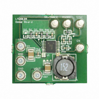
LM20134EVAL
Manufacturer Part Number
LM20134EVAL
Description
BOARD EVAL 4A POWERWISE LM20134
Manufacturer
National Semiconductor
Series
PowerWise®r
Specifications of LM20134EVAL
Main Purpose
DC/DC, Step Down
Outputs And Type
1, Non-Isolated
Voltage - Output
1.2V
Current - Output
4A
Voltage - Input
2.95 ~ 5.5V
Regulator Topology
Buck
Board Type
Fully Populated
Utilized Ic / Part
LM20134
Lead Free Status / RoHS Status
Not applicable / Not applicable
Power - Output
-
Frequency - Switching
-


Oscillator and Clock Synchronization
Error Amplifier and Modulator
Power Good
Absolute Maximum Ratings
If Military/Aerospace specified devices are required,
please contact the National Semiconductor Sales Office/
Distributors for availability and specifications.
Electrical Characteristics
Limits in standard type are for T
+125°C. Minimum and Maximum limits are guaranteed through test, design, or statistical correlation. Typical values represent the
most likely parametric norm at T
ΔV
Voltages from the indicated pins to GND
AVIN, PVIN, EN, PGOOD, SS/
TRK, COMP, FB, SW, SYNC
Storage Temperature
Junction Temperature
V
T
I
I
V
V
T
COMP_SRC
COMP_SNK
Symbol
V
R
R
V
T
UVLO_HYS
V
CL_BLANK
OUT
DC
F
OVP_HYS
V
V
F
ON_TIME
IH_SYNC
IL_SYNC
I
V
F
A
V
PGOOD
PGHYS
DS_ON
DS_ON
TRACK
SYNC
V
OSCH
I
UVLO
OSCL
PGTH
I
I
I
I
g
I
I
VCC
OSC
OVP
SD
VOL
OH
CL
SS
FB
OL
FB
Q
MAX
m
/ΔI
OUT
Parameter
Feedback pin voltage
Load Regulation
Switch Current Limit Threshold
High-Side Switch On Resistance
Low-Side Switch On Resistance
Operating Quiescent Current
Shutdown Quiescent current
VIN Under Voltage Lockout
VIN Under Voltage Lockout Hysteresis
VCC Voltage
Soft-Start Pin Source Current
SS/TRK Accuracy, V
Oscillator Frequency
Maximum SYNC Frequency
Minimum SYNC Frequency
SYNC pin Logic High
SYNC pin Logic Low
SYNC pin input leakage
Maximum Duty Cycle
Minimum On Time
Current Sense Blanking Time
Feedback pin bias current
COMP Output Source Current
COMP Output Sink Current
Error Amplifier Transconductance
Error Amplifier Voltage Gain
Over Voltage Protection Rising Threshold
Over Voltage Protection Hysteresis
PGOOD Rising Threshold
PGOOD Falling Hysteresis
PGOOD deglitch time
PGOOD Low Sink Current
PGOOD High Leakage Current
J
J
= 25°C only, limits in bold face type apply over the junction temperature (T
= 25°C, and are provided for reference purposes only.
SS
- V
FB
-65°C to 150°C
Unless otherwise stated, the following conditions apply: AVIN = PVIN = VIN = 5V.
-0.3V to +6V
(Note 1)
150°C
Conditions
V
I
V
I
I
Non-switching, V
V
Rising V
Falling V
I
V
V
V
V
I
After Rising V
V
V
V
I
With respect to V
With respect to V
V
V
3
OUT
SW
SW
VCC
LOAD
COMP
IN
IN
EN
SS/TRK
SS/TRK
SYNC
SYNC
FB
FB
FB
PGOOD
PGOOD
= 2.95V to 5.5V
= 3.3V
= 3.5A
= 3.5A
= 0.8V
= V
= 1.0V, V
= 0V
PVIN, AVIN to GND
Junction Temperature
Operating Ratings
= 100 mA to 4A
= 0 µA
Power Dissipation (Note 2)
Lead Temperature (Soldering,
10 sec)
Minimum ESD Rating (Note 3)
= 0A
= ± 50 µA
= Static
= 5V
COMP
= 0V
= 0.4V
= 0.4V
= 5V
IN
IN
= 0.6V
COMP
SW
FB
FB
FB
= 0.6V
= V
COMP
0.788
2.45
2.45
Min
360
460
450
105
-10
5.8
0.6
80
80
92
2
2
J
) range of -40°C to
1500
2000
0.08
Typ
410
100
100
100
510
108
0.8
6.4
3.5
2.7
2.7
4.5
36
32
90
45
10
85
80
94
16
−40°C to + 125°C
3
1
2
2
1
5
2.95V to 5.5V
0.812
www.national.com
Max
2.95
2.95
180
100
460
100
600
111
100
7.9
0.8
55
52
15
96
6
7
3
3
260°C
2.6W
±2kV
µmho
Unit
%/A
kHz
kHz
kHz
mΩ
mΩ
mA
mV
mV
V/V
mA
µA
µA
nA
nA
µA
µA
nA
ns
ns
µs
%
%
%
%
%
V
A
V
V
V
V
Related parts for LM20134EVAL
Image
Part Number
Description
Manufacturer
Datasheet
Request
R

Part Number:
Description:
MODULE TXRX BLUETOOTH 2 18SMD
Manufacturer:
Flexipanel
Datasheet:

Part Number:
Description:
MODULE TXRX BLUETOOTH 2 18DIP
Manufacturer:
Flexipanel
Datasheet:

Part Number:
Description:
LM20 2.4V, 10?A, SC70, micro SMD Temperature Sensor
Manufacturer:
National Semiconductor
Datasheet:
Part Number:
Description:
National Semiconductor [8-Bit D/A Converter]
Manufacturer:
National Semiconductor
Datasheet:
Part Number:
Description:
National Semiconductor [Media Coprocessor]
Manufacturer:
National Semiconductor
Datasheet:
Part Number:
Description:
Digitally Controlled Tone and Volume Circuit with Stereo Audio Power Amplifier, Microphone Preamp Stage and National 3D Sound
Manufacturer:
National Semiconductor
Datasheet:
Part Number:
Description:
Digitally Controlled Tone and Volume Circuit with Stereo Audio Power Amplifier, Microphone Preamp Stage and National 3D Sound
Manufacturer:
National Semiconductor
Datasheet:
Part Number:
Description:
AC97 Rev 2 Codec with Sample Rate Conversion and National 3D Sound
Manufacturer:
National Semiconductor
Part Number:
Description:
Manufacturer:
National Semiconductor
Datasheet:
Part Number:
Description:
Manufacturer:
National Semiconductor
Datasheet:
Part Number:
Description:
General Purpose, Low Voltage, Low Power, Rail-to-Rail Output Operational Amplifiers
Manufacturer:
National Semiconductor
Datasheet:
Part Number:
Description:
8-bit 20 MSPS flash A/D converter.
Manufacturer:
National Semiconductor
Datasheet:
Part Number:
Description:
Low Noise Quad Operational Amplifier
Manufacturer:
National Semiconductor
Datasheet:
Part Number:
Description:
Quad Differential Line Receivers
Manufacturer:
National Semiconductor
Datasheet: