LM20145EVAL National Semiconductor, LM20145EVAL Datasheet - Page 14
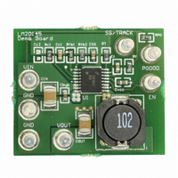
LM20145EVAL
Manufacturer Part Number
LM20145EVAL
Description
BOARD EVAL 5A POWERWISE LM20145
Manufacturer
National Semiconductor
Series
PowerWise®r
Specifications of LM20145EVAL
Main Purpose
DC/DC, Step Down
Outputs And Type
1, Non-Isolated
Voltage - Output
1.2V
Current - Output
5A
Voltage - Input
2.95 ~ 5.5V
Regulator Topology
Buck
Frequency - Switching
500kHz
Board Type
Fully Populated
Utilized Ic / Part
LM20145
Lead Free Status / RoHS Status
Not applicable / Not applicable
Power - Output
-


www.national.com
The power stage transfer function is dictated by the modula-
tor, output LC filter, and load; while the feedback transfer
function is set by the feedback resistor ratio, error amp gain,
and external compensation network.
To achieve a -20dB/decade slope, the error amplifier zero,
located at f
pole (f
can be added to cancel the output filter zero at f
cellation of the output filter zero is recommended if larger
value, non-ceramic output capacitors are used.
Compensation of the LM20144 is achieved by adding an RC
network as shown in Figure 5 below.
A good starting value for C
Once the value of C
calculated using the equation below to cancel the output filter
pole (F
FIGURE 5. Compensation Network for LM20145
P(FIL)
P(FIL)
FIGURE 4. LM20145 Loop Compensation
). An additional error amp pole, located at f
Z(EA)
) as shown in Figure 4.
, should positioned to cancel the output filter
C1
is chosen the value of RC should be
C1
for most applications is 4.7 nF.
30030714
Z(FIL)
30030713
. Can-
P2(EA)
,
14
A higher crossover frequency can be obtained, usually at the
expense of phase margin, by lowering the value of C
recalculating the value of R
recalculating R
lower crossover frequency. As with any attempt to compen-
sate the LM20145 the stability of the system should be verified
for desired transient droop and settling time.
If the output filter zero, F
quency (F
at the COMP pin to ground. This capacitor adds a pole to
cancel the output filter zero assuring the crossover frequency
will occur before the double pole at f
margin. The output filter zero is set by the output capacitor
value and ESR as shown in the equation below.
If needed, the value for C
equation shown below.
Where R
R
AVIN FILTERING COMPONENTS (C
To prevent high frequency noise spikes from disturbing the
sensitive analog circuitry connected to the AVIN and AGND
pins, a high frequency RC filter is required between PVIN and
AVIN. These components are shown in Figure 2. as C
R
ommended value of C
should be placed as close to the IC as possible with a direct
connection from AVIN to AGND. A good quality X5R or X7R
ceramic capacitor should be used for C
SUB-REGULATOR BYPASS CAPACITOR (C
The capacitor at the VCC pin provides noise filtering and sta-
bility for the internal sub-regulator. The recommended value
of C
10 µF. The capacitor should be a good quality ceramic X5R
or X7R capacitor. In general, a 1 µF ceramic capacitor is rec-
ommended for most applications.
SETTING THE START UP TIME (C
The addition of a capacitor connected from the SS pin to
ground sets the time at which the output voltage will reach the
final regulated value. Larger values for C
start up times. Table 3, shown below provides a list of soft
start capacitors and the corresponding typical start up times.
C1
F
. The required value for R
VCC
is the calculated compensation resistance.
TABLE 3. Start Up Times for Different Soft-Start
Start Up Time (ms)
should be no smaller than 1 µF and no greater than
ESR
C
), an additional capacitor (C
is the output capacitor series resistance and
10
15
20
1
5
C1
will provide additional phase margin at a
F
Capacitors
Z(FIL)
is 1.0 µF. The filter capacitor, C
C2
C1
F
should be calculated using the
. Likewise, increasing C
approaches the crossover fre-
is 1Ω. C
SW
SS
F
/2 degrades the phase
)
F
F
C2
and R
SS
.
must be used. Rec-
C
) should be placed
will result in longer
SS
none
100
120
33
68
(nF)
F
)
VCC
)
C1
C1
F
and
and
and
F
Related parts for LM20145EVAL
Image
Part Number
Description
Manufacturer
Datasheet
Request
R

Part Number:
Description:
MODULE TXRX BLUETOOTH 2 18SMD
Manufacturer:
Flexipanel
Datasheet:

Part Number:
Description:
MODULE TXRX BLUETOOTH 2 18DIP
Manufacturer:
Flexipanel
Datasheet:

Part Number:
Description:
LM20 2.4V, 10?A, SC70, micro SMD Temperature Sensor
Manufacturer:
National Semiconductor
Datasheet:
Part Number:
Description:
National Semiconductor [8-Bit D/A Converter]
Manufacturer:
National Semiconductor
Datasheet:
Part Number:
Description:
National Semiconductor [Media Coprocessor]
Manufacturer:
National Semiconductor
Datasheet:
Part Number:
Description:
Digitally Controlled Tone and Volume Circuit with Stereo Audio Power Amplifier, Microphone Preamp Stage and National 3D Sound
Manufacturer:
National Semiconductor
Datasheet:
Part Number:
Description:
Digitally Controlled Tone and Volume Circuit with Stereo Audio Power Amplifier, Microphone Preamp Stage and National 3D Sound
Manufacturer:
National Semiconductor
Datasheet:
Part Number:
Description:
AC97 Rev 2 Codec with Sample Rate Conversion and National 3D Sound
Manufacturer:
National Semiconductor
Part Number:
Description:
Manufacturer:
National Semiconductor
Datasheet:
Part Number:
Description:
Manufacturer:
National Semiconductor
Datasheet:
Part Number:
Description:
General Purpose, Low Voltage, Low Power, Rail-to-Rail Output Operational Amplifiers
Manufacturer:
National Semiconductor
Datasheet:
Part Number:
Description:
8-bit 20 MSPS flash A/D converter.
Manufacturer:
National Semiconductor
Datasheet:
Part Number:
Description:
Low Noise Quad Operational Amplifier
Manufacturer:
National Semiconductor
Datasheet:
Part Number:
Description:
Quad Differential Line Receivers
Manufacturer:
National Semiconductor
Datasheet: