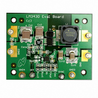
LM3430EVAL/NOPB National Semiconductor, LM3430EVAL/NOPB Datasheet
LM3430EVAL/NOPB
Specifications of LM3430EVAL/NOPB


Related parts for LM3430EVAL/NOPB

LM3430EVAL/NOPB Summary of contents
Page 1
... The LM3430 is available in the LLP-12 package. Typical Application © 2007 National Semiconductor Corporation Features ■ Internal 40V Startup Regulator ■ 1A Peak MOSFET Gate Driver ■ ...
Page 2
Connection Diagram Ordering Information Part Number LM3430SD LM3430SDX Pin Descriptions Pin(s) Name Description 1 VDHC Proprietary control input from LM3432 2 VIN Source input voltage 3 FB Feedback pin Error amplifier output and PWM 4 COMP comparator input Output of ...
Page 3
... Absolute Maximum Ratings If Military/Aerospace specified devices are required, please contact the National Semiconductor Sales Office/ Distributors for availability and specifications. VIN to GND VCC to GND RT/SYNC to GND OUT to GND All other pins to GND Power Dissipation Junction Temperature Electrical Characteristics junction temperature (T ) range of -40°C to +125°C. Minimum and Maximum limits are guaranteed through test, design, or statistical J correlation ...
Page 4
Symbol Parameter SOFT-START I Soft-start Current Source SS V Soft-start to COMP Offset SS-OFF OSCILLATOR RT to GND = 84.5 kΩ GND = 27.4 kΩ GND = 16.2 kΩ V Synchronization Rising Threshold SYNC-HI ...
Page 5
Typical Performance Characteristics Efficiency 40V 25° Max Duty Cycle vs 20209654 20209604 = 25° 20209606 5 V vs. Temp (V = 18V) FB ...
Page 6
R vs OUT Pin t vs. Gate Capacitance R www.national.com = 25°C) 20209608 20209610 6 SS vs. Temperature 20209609 OUT Pin t vs. Gate Capacitance F 20209611 ...
Page 7
Block Diagram 7 20209612 www.national.com ...
Page 8
Example Circuit: LM3430 and LM3432 Application Parameters for Various LED Configurations Input Voltage 8V to 21V Maximum Output 33V Voltage LED Configuration 8 LEDs x 6 Strings per string Switching Frequency 1 MHz L1 22 µ ...
Page 9
Cin 10 µF, 50V Cinx 100 nF Css 16.5 kΩ Rfb1 4.64 kΩ Rfb2 118 kΩ Ruv1 10 kΩ Ruv2 49.9 kΩ Control Loop Compensation kΩ C2 220 nF VDHC Rdhc 30 ...
Page 10
FIGURE 2. Enable/Disable Using UVLO ERROR AMPLIFIER An internal high gain error amplifier is provided within the LM3430. The amplifier’s non-inverting input is internally set to a fixed reference voltage of 1.25V. The inverting input is con- nected to the ...
Page 11
In addition to preventing sub-harmonic oscillation, increasing the amplitude of the compensation ramp voltage decreases the voltage across R required to trip the current limit com- SNS parator. This technique can be used to lower the value of R and ...
Page 12
Conduction loss approximately: C The factor 1.3 accounts for the increase in MOSFET on re- sistance due to heating. Alternatively, the factor of 1.3 can be ignored and the on resistance of the ...
Page 13
Inductance for Minimum Input Voltage D = (33 – 9.0 – 0.5) / (33 – 0.5) = 72% VIN(MIN 0. – 0.72) = 0.64A L-VIN(MIN) Δi = 0.4 x 0.64A = 0.26A L Inductance for Maximum ...
Page 14
FIGURE 5. ΔV Using High ESR Capacitors O FIGURE 6. ΔV Using Low ESR Capacitors O For this example, the load is fairly constant, and the height restriction favors the low profile of ceramic capacitors. The output ripple voltage waveform ...
Page 15
In general, the requirement for greatest capacitance comes from the power supply interaction. The inductance and resistance of the input source must be estimated, and if this information is not available, they can ...
Page 16
One popular method for selecting the compensation compo- nents is to create Bode plots of gain and phase for the power stage and error amplifier. Combined, they make the overall bandwidth and phase margin of the regulator easy to deter- ...
Page 17
RHP zero and the sampling double pole. The effect of the ESR zero is not seen because its frequency is several decades above the switching frequency. The combination of increasing gain and decreasing phase makes converters with RHP zeroes difficult ...
Page 18
FIGURE 9. Error Amplifier Gain and Phase 12. Plot or evaluate the complete control loop transfer function: The complete control loop transfer function is ob- tained by multiplying the power stage and error amplifier functions together. The bandwidth and phase ...
Page 19
The gate driving loss term from the power MOSFET section of Design Considerations is included in the chip operating loss. For the LM3430 equal to the steady state operating IN current plus the MOSFET driving current, ...
Page 20
SENSE LINES The top of R should be connected to the CS pin with a SNS separate trace made as short as possible. Route this trace away from the inductor and the switch node (where D1, Q1, and L1 connect). ...
Page 21
BOM for Example Circuit ID Part Number U1 LM3430 Low-Side Controller Q1 Si4850EY D1 CMHSH5-4 L1 SLF7045T-470M90-1P F Cin C3216X7R1E335M Co C3216X7R1H105M Cf C2012X7R1E105K Cinx VJ0805Y104KXXAT Cox C1 VJ0805A391KXXAT C2 VJ0805Y393KXXAT Css VJ0805Y103KXXAT Ccs VJ0805Y102KXXAT R1 CRCW08052001F Rfb1 CRCW08057870F Rfb2 ...
Page 22
Physical Dimensions www.national.com inches (millimeters) unless otherwise noted 12-Lead LLP Package NS Package Number SDF12A 22 ...
Page 23
Notes 23 www.national.com ...
Page 24
... National Semiconductor and the National Semiconductor logo are registered trademarks of National Semiconductor Corporation. All other brand or product names may be trademarks or registered trademarks of their respective holders. ...