KIT34700EPEVBE Freescale Semiconductor, KIT34700EPEVBE Datasheet
KIT34700EPEVBE
Specifications of KIT34700EPEVBE


Related parts for KIT34700EPEVBE

KIT34700EPEVBE Summary of contents
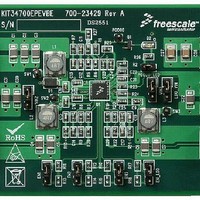
Page 1
... EN1 Enable 4 EN_LDO AGND GND2 GND3 Freescale Semiconductor, Inc. reserves the right to change the detail specifications, as may be required, to permit improvements in the design of its products. © Freescale Semiconductor, Inc., 2009. All rights reserved. Device MC34700EP/R2 Features • Three switching regulators: 2 synchronous and 1 non- synchronous • ...
Page 2
... Regulator Control AGND Feed Bootstrap Forward BST1 Circuit VIN1 Gate Drive SW1 COMP1 FB1 Bootstrap BST2 Circuit VIN2 SW2 Gate Drive GND2 COMP2 FB2 Bootstrap BST3 Circuit VIN3 SW3 Gate Drive GND3 COMP3 FB3 Analog Integrated Circuit Device Data Freescale Semiconductor ...
Page 3
... Temperature and Moisture Sensitivity Levels (MSL www.freescale.com, search by part number [e.g. remove prefixes/suffixes and enter the core ID to view all orderable parts. (i.e. MC33xxxD enter 33xxx), and review parametrics. Analog Integrated Circuit Device Data Freescale Semiconductor ELECTRICAL CHARACTERISTICS ABSOLUTE MAXIMUM RATINGS ...
Page 4
... EN_IN t - 1.0 - DELAY1 t - 160 - DELAY2,3 V 0.690 0.700 0.710 REF1,2,3 V 0.690 0.700 0.710 REF_LDO f 760 800 840 SW t 2.5 3.5 4.5 SS_BUCKREG t 0.3 0.5 0.7 SS_LDO Analog Integrated Circuit Device Data Freescale Semiconductor Unit Ω V V/μs μF μ MΩ kHz ms ms ...
Page 5
... Error Amplifier DC Gain Error Amplifier Unity-gain Bandwidth Error Amplifier Slew Rate @ 15 pF Current Limit Timer Current Limit Retry Timeout Period Analog Integrated Circuit Device Data Freescale Semiconductor STATIC AND DYNAMIC ELECTRICAL CHARACTERISTICS ≤ 40°C ≤ T ≤ 85°C, GND = 0 V, unless otherwise noted. Typical 25° ...
Page 6
... DC3MAX ΔV -1.5 - 1.5 OUT3 I 2.0 - 4.5 SHORT3 - 160 - DS(ON)_HS - 140 - DS(ON)_LS R - 150 - 400 - SW3 A - 110 - EA GBW - 4 1 LIM3 - 100 - TIMEOUT3 Analog Integrated Circuit Device Data Freescale Semiconductor Unit mΩ mΩ mΩ μA dB MHz V/μ mΩ mΩ mΩ μA dB MHz V/μ ...
Page 7
... THERMAL SHUTDOWN Maximum Thermal Shutdown Threshold Typical Thermal Shutdown Threshold Minimum Thermal Shutdown Threshold Thermal Shutdown Hysteresis Analog Integrated Circuit Device Data Freescale Semiconductor STATIC AND DYNAMIC ELECTRICAL CHARACTERISTICS ≤ 40°C ≤ T ≤ 85°C, GND = 0 V, unless otherwise noted. Typical 25°C under nominal conditions, unless otherwise noted. ...
Page 8
... This input enables buck regulator #2. Asserting EN2 high turns on DC/DC #2. The internal control logic remains active as long as VIN is present. 34700 8 PIN CONNECTIONS SW1 2 23 SW1 TRANSPARENT TOP VIEW 5 20 PIN 33 SW2 Figure 3. 34700 Pin Connections FUNCTIONAL PIN DESCRIPTIONS Pin Description VIN LDO_VIN LDO LDO_FB GND3 SW3 VIN3 BST3 Analog Integrated Circuit Device Data Freescale Semiconductor ...
Page 9
... Buck regulator #1’s compensation output. COMP1 is connected to DC/DC #1’s error amplifier’s output. Connect the required external compensation network between the COMP1 pin and the FB1 pin. 33 AGND Thermal pad for heat transfer. Connect the thermal pad to the analog ground. Analog Integrated Circuit Device Data Freescale Semiconductor FUNCTIONAL PIN DESCRIPTIONS Pin Description PIN CONNECTIONS 34700 9 ...
Page 10
... LDO Iout (A) Figure 4. Typical LDO Efficiency CH1 Loop Response 180 135 90 Phase 45 0 -45 -90 -135 -180 1.0E+3 10.0E+3 100.0E+3 1.0E+6 Frequency (Hz) CH2 Loop Response 180 Phase 135 -45 -90 -135 -180 1.0E+3 10.0E+3 100.0E+3 1.0E+6 Frequency (Hz) Analog Integrated Circuit Device Data Freescale Semiconductor ...
Page 11
... EN1 COMP1 VOUT1 SW1 12 VIN1, 3.4 VOUT1@ 1.5 A Figure 8. EN CH1 Start-up EN2 COMP2 VOUT2 SW2 3.4 VIN2, 2.5 VOUT1@ 1.25 A Figure 9. EN CH2 Start-up Analog Integrated Circuit Device Data Freescale Semiconductor 180 EN3 135 90 45 COMP3 0 VOUT3 -45 -90 SW3 -135 -180 1 ...
Page 12
... VIN2, 2.47 VOUT2 1.25 A transient Figure 16. CH2 Transient Response IOUT3-1.0A/div VOUT3 COMP3 SW3 5 VIN3, 1.28 VOUT3 1.25 A transient Figure 17. CH3 Transient Response IOUT_LDO3-250mA/div VOUT_LDO VIN_LDO 1.5 VIN_LDO, 0.9 VOUT_LDO 400mA transient Figure 18. LDO Transient Response Analog Integrated Circuit Device Data Freescale Semiconductor ...
Page 13
... IC from overstress. The response of the 34700 to a fault condition is described as follows. Analog Integrated Circuit Device Data Freescale Semiconductor INITIALIZATION faster than the control loop can typically respond, resulting in overshoot result, the soft start periods for the switching regulators are longer (3 ...
Page 14
... V IN Figures 19 thru 21. Buck Converter 1 2.0 to 5.25 V OUT 1.5 A MAX Buck Converter 2 0.7 to 3.6 V OUT 1.25 A MAX Buck Converter 3 0.7 to 3.6 V OUT 1.25 A MAX LDO 0.7 to 3.6 V OUT 400 mA MAX Figure 19. General Configuration Analog Integrated Circuit Device Data Freescale Semiconductor ...
Page 15
... Where η is the estimated efficiency of the buck converters, use 0.85 for the initial estimate. Analog Integrated Circuit Device Data Freescale Semiconductor When making the power calculations, be sure to include any input currents from regulators that are connected to the converter as part of the output current. For example, the input 2 ...
Page 16
... To do this an understanding of the major current carrying loops is R5 VOUT3 LDO_EN LDO R6 t Analog Integrated Circuit Device Data Freescale Semiconductor ...
Page 17
... V = 0.7 V REF Analog Integrated Circuit Device Data Freescale Semiconductor The use of a multi-layer printed circuit board is recommended. Dedicate one layer, usually the layer under the top layer ground plane. Make all critical component ground connections with vias to this layer. Make sure that the ...
Page 18
... N × OUT ( MAX ) = C OUT Δ where the maximum output voltage overshoot − IN(MAX) OUT × × OUT IN(MAX) SW Δ OUT(MAX PEAK ( ) − Δ OUT OUT Analog Integrated Circuit Device Data Freescale Semiconductor ...
Page 19
... N- MOSFET. This capacitor develops a floating voltage supply Analog Integrated Circuit Device Data Freescale Semiconductor which is referenced to the switch node (SW) or the source of the high side MOSFET. The bootstrap capacitor is charged every cycle, when the low side MOSFET or the catch diode ...
Page 20
... P2 R TOP ⎞ f ⎟ ⎟ − × ⎠ × × ⋅ ⎞ ⎛ ⎞ ⋅ ⎟ ⎜ ⎜ ⎟ ⎟ ⋅ ⋅ R COMP 2 ⎟ COMP + C C ⎝ ⎠ ⎠ COMP 2 Analog Integrated Circuit Device Data Freescale Semiconductor ) at Z2 ...
Page 21
... The open loop error amplifier gain bounds the compensation gain. Check the compensation gain whichever is greater, against the capabilities of the P2 error amplifier. For reference, the equations for the compensation break frequencies are given Analog Integrated Circuit Device Data Freescale Semiconductor = ...
Page 22
... APPLICATION EXAMPLE 34700 22 APPLICATION EXAMPLE COMP3 VGREG FB3 VDDI EN_LDO PGOOD EN3 AGND EN2 VOUT1 FB1 EN1 FB2 COMP1 VIN1 COMP2 Figure 26. 34700 Typical Application Analog Integrated Circuit Device Data Freescale Semiconductor ...
Page 23
... Freescale does not assume liability, endorse, or warrant components from external manufacturers that are referenced in circuit drawings or tables. While Freescale offers component recommendations in this configuration the customer’s responsibility to validate their application. Analog Integrated Circuit Device Data Freescale Semiconductor BILL OF MATERIAL Table 1. MC34700 Bill of Material ...
Page 24
... APPLICATION EXAMPLE PACKAGE DIMENSIONS For the most current package revision, visit www.freescale.com and perform a “keyword” search using the 98AXXXXXXXX listed. 34700 24 PACKAGE DIMENSIONS EP SUFFIX (Pb FREE) 32-PIN 98ASA10800D REVISION D Analog Integrated Circuit Device Data Freescale Semiconductor ...
Page 25
... Analog Integrated Circuit Device Data Freescale Semiconductor EP SUFFIX (Pb FREE) 32-PIN 98ASA10800D REVISION D APPLICATION EXAMPLE PACKAGE DIMENSIONS 34700 25 ...
Page 26
... APPLICATION EXAMPLE PACKAGE DIMENSIONS 34700 26 EP SUFFIX (Pb FREE) 32-PIN 98ASA10800D REVISION D Analog Integrated Circuit Device Data Freescale Semiconductor ...
Page 27
... Changed category from “Advance Information” to “Technical Data” 4.0 • Converted the datasheet to the PMMIC format 6/2009 5.0 • Added waveforms Analog Integrated Circuit Device Data Freescale Semiconductor INTERNAL REVISION HISTORY MC34700 Simplified Application Diagram on page 1 INTERNAL REVISION HISTORY PACKAGE DIMENSIONS 34700 27 ...
Page 28
... Freescale Semiconductor was negligent regarding the design or manufacture of the part. Freescale™ and the Freescale logo are trademarks of Freescale Semiconductor, Inc ...