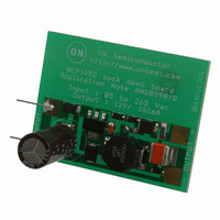
NCP1052GEVB ON Semiconductor, NCP1052GEVB Datasheet

EVAL BOARD FOR NCP1052G

NCP1052GEVB

Manufacturer Part Number
NCP1052GEVB
Description
EVAL BOARD FOR NCP1052G
Manufacturer
ON Semiconductor
Datasheets

Specifications of NCP1052GEVB

Design Resources
NCP1052 Eval Board BOM NCP1052GEVB Gerber Files NCP1052 Demo Board Schematic
Main Purpose
AC/DC, Non-Isolated
Outputs And Type
1, Non-Isolated
Power - Output
1.2W
Voltage - Output
120V
Current - Output
100mA
Voltage - Input
85 ~ 265VAC
Regulator Topology
Boost, Buck
Frequency - Switching
136kHz
Board Type
Fully Populated
Utilized Ic / Part
NCP1052
Lead Free Status / RoHS Status
Lead free / RoHS Compliant
For Use With/related Products
NCP1052G
Other names
NCP1052GEVBOS
AND8098/D
Low−Cost 100 mA
High−Voltage Buck and
Buck−Boost Using NCP1052
Prepared by: Kahou Wong
ON Semiconductor
100 mA non-isolated power supply using NCP1052 by
buck and buck-boost topology. The NCP1052 is one of the
latest low-cost switching controllers with integrated 700 V/
300 mA power switch from ON Semiconductor. It is
primarily designed for isolated 10 W-range flyback
converter. If isolation is not needed, the IC can also be used
as stepping-down buck and buck-boost converter for
further cost saving by removing optocoupler and replacing
the transformer by an inductor. The output current capability
is 100 mA. The possible operating range is from input range
between 20 Vdc and 700 Vdc to output range of 5.0 V or
above with 100 mA. Typical efficiency around 65% is
obtained in the 12 V buck demo board.
similar to each other. Their major difference is that buck
provides a positive output voltage but buck-boost provides
a negative output voltage referring to the input ground.
June, 2003 - Rev. 1
This application note presents low-cost high-voltage
Advantages of the proposed circuits include:
The proposed buck and buck-boost converters are very
Comparing to flyback, buck and buck-boost eliminates
optocoupler and replaces transformer by an inductor for
cost saving.
Buck and buck-boost offers smaller voltage stress in
switches comparing to flyback. It minimizes the
switching loss and increases efficiency.
NCP105x can power up itself from the high input
voltage with wide range between 20 Vdc and 700 Vdc.
It needs no extra supply circuit.
NCP105x operates at 44, 100, or 136 kHz and
accommodates low-cost components such as aluminum
electrolytic capacitors and powered-iron core magnetic.
NCP105x offers frequency jittering for reduced
electromagnetic inference (EMI).
NCP105x offers thermal and short circuit fault
protection.
Simple design as no control-loop compensation is
concerned.
Semiconductor Components Industries, LLC, 2003
INTRODUCTION
1
converters. The rectifier circuit, which consists of capacitor
C
voltage. Then, the NCP1052 is self-powered up from the
rectified input voltage directly with a V
When the switch inside the IC is opened, there is a voltage
across Drain (D) and Source (S) pins of the IC. If this voltage
is greater than 20 V, an internal current source I
(typ.) inside the IC charges up C
up for the operation of the IC. Comparing to the switching
frequency, the V
7.5-8.5 V hysteresis loop. This V
frequency jittering features to minimize EMI and
short-circuit fault timing function.
voltage powers up the IC through the path across the
inductor L and capacitor C. This charging path passes
Input
Input
3
Figure 1 shows the proposed buck and buck-boost
In Figure 2a it is noted that in the buck topology the input
and diode D
D
Figure 1. Proposed Circuit Using NCP1052
3
D
C
3
3
D
C
V
PRINCIPLE OF OPERATION
D
3
FB
CC
V
FB
CC
3
CC
, is in the front end for AC or DC input
D
C
APPLICATION NOTE
2
D
2
voltage level is in a lower-frequency
C
S
2
(b) Buck-boost
Z
2
S
2
Z
http://onsemi.com
2
(a) Buck
L
C
1
D
C
D
D
2
1
1
D
R
and a voltage in C
1
CC
Publication Order Number:
1
L
R
hysteresis loop is for
1
C
C
CC
Z
Z
capacitor C
start
1
1
AND8098/D
= 6.3 mA
2
Output
Output
is built
2
.

Related parts for NCP1052GEVB

NCP1052GEVB Summary of contents

Page 1

... NCP1052 by buck and buck-boost topology. The NCP1052 is one of the latest low-cost switching controllers with integrated 700 V/ 300 mA power switch from ON Semiconductor primarily designed for isolated 10 W-range flyback converter. If isolation is not needed, the IC can also be used as stepping-down buck and buck-boost converter for further cost saving by removing optocoupler and replacing the transformer by an inductor ...

Page 2

Hence, the value of C small enough to increase this charging frequency f order to reduce output voltage ripple because some efficiency is lost due to ...

Page 3

Hence, a zener diode Z “dummy” load resistor is needed to consume the minimum amount of energy as shown in Figure also noted that when ...

Page 4

In non-isolated topologies such as buck or buck-boost, the circuits are mainly designed for CCM. The CCM burst-mode waveform is different to the PWM waveform in Figure 5. Because of this characteristic, burst mode requires a higher peak value of ...

Page 5

NCP1052 will have a very high current limit effectively because there is a propagation delay (typically 135 ns) to turn off the switch. The current flowing through the inductor L includes three ...

Page 6

The proposed buck-boost is better in term of the standby ability because the V charging current in Figure 2(b) CC only passes through the inductor. The charging current pulses become an averaged energy stored in the inductor and ...

Page 7

... Description Switching Regulator 1A 600V ultrafast General diode 1A 600V standard recovery 12V 5% zener 6.8V 5% zener 2 k 220 tantalum 0. ceramic 6.8 F, 16V, tantalum 400V 10 F 680 H http://onsemi.com 7 Manufacturer ON Semiconductor ON Semiconductor ON Semiconductor ON Semiconductor ON Semiconductor ON Semiconductor Vishay Vishay Vishay Vishay Rubycon Cooper ...

Page 8

V = 300 Vdc V = 100 Vdc 100 150 200 OUTPUT CURRENT (mA) (a) Load Regulation 200 ...

Page 9

Output 2 with 150 mA -5 -10 -15 -20 Output 1 with 200 mA -25 50 100 150 200 INPUT VOLTAGE (Vac) Figure 12. Line Regulation of the Dual Output Buck-boost AND8098/D 100 mA high-voltage low-cost buck and buck-boost ...

Page 10

... Fax: 303-675-2176 or 800-344-3867 Toll Free USA/Canada Email: ONlit@hibbertco.com N. American Technical Support: 800-282-9855 Toll Free USA/Canada AND8098/D JAPAN: ON Semiconductor, Japan Customer Focus Center 2-9-1 Kamimeguro, Meguro-ku, Tokyo, Japan 153-0051 Phone: 81-3-5773-3850 ON Semiconductor Website: http://onsemi.com For additional information, please contact your local Sales Representative ...

Related keywords