LM2595ATPBCKGEVB ON Semiconductor, LM2595ATPBCKGEVB Datasheet - Page 4
LM2595ATPBCKGEVB
Manufacturer Part Number
LM2595ATPBCKGEVB
Description
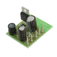
EVAL BOARD FOR LM2595ATPBCKG
Manufacturer
ON Semiconductor
Specifications of LM2595ATPBCKGEVB
Design Resources
LM2595ATPBCKGEVB BOM LM2595ATPBCKGEVB Gerber Files LM2595ATPBCKGEVB Schematic
Main Purpose
DC/DC, Step Down
Outputs And Type
1, Non-Isolated
Voltage - Output
5V
Current - Output
1A
Voltage - Input
4.5 ~ 40 V
Regulator Topology
Buck
Frequency - Switching
150kHz
Board Type
Fully Populated
Utilized Ic / Part
LM2595
Lead Free Status / RoHS Status
Lead free / RoHS Compliant
Power - Output
-
Lead Free Status / Rohs Status
Lead free / RoHS Compliant
For Use With/related Products
LM2595ATPBCKG
Other names
LM2595ATPBCKGEVBOS


1. External components such as the catch diode, inductor, input and output capacitors can affect switching regulator system performance.
2. The oscillator frequency reduces to approximately 30 kHz in the event of an output short or an overload which causes the regulated output
3. No diode, inductor or capacitor connected to output (Pin 1) sourcing the current.
4. Feedback (Pin 4) removed from output and connected to 0 V.
5. Feedback (Pin 4) removed from output and connected to +12 V to force the output transistor “off”.
6. V
SYSTEM PARAMETERS
ELECTRICAL CHARACTERISTICS
over full Operating Temperature Range −40°C to +125°C
LM2595 (Note 1, Test Circuit Figure 16)
ON/OFF PIN LOGIC INPUT
ON/OFF Pin Input Current
Feedback Voltage (V
Feedback Voltage (8.0 V ≤ V
Efficiency (V
Feedback Bias Current (V
Oscillator Frequency (Note 2)
Saturation Voltage (I
Max Duty Cycle “ON” (Note 4)
Current Limit (Peak Current, Notes 2 and 3)
Output Leakage Current (Notes 5 and 6)
Output = 0 V
Output = −1.0 V
Quiescent Current (Note 5)
Standby Quiescent Current (ON/OFF Pin = 5.0 V (“OFF”))
(Note 6)
Threshold Voltage
V
V
ON/OFF Pin = 5.0 V (Regulator OFF)
ON/OFF Pin = 0 V (regulator ON)
out
out
When the LM2595 is used as shown in the Figure 16 test circuit, system performance will be as shown in system parameters section.
voltage to drop approximately 40% from the nominal output voltage. This self protection feature lowers the average dissipation of the IC by
lowering the minimum duty cycle from 5% down to approximately 2%.
in
= 0 V (Regulator OFF)
= Nominal Output Voltage (Regulator ON)
= 40 V.
in
= 12 V, I
out
in
Load
= 12 V, I
= 1.0 A, Notes 3 and 4)
out
= 1.0 A, V
in
= 5.0 V)
Characteristics
Characteristics
≤ 40 V, 0.2 A ≤ I
Load
= 0.2 A, V
out
= 5.0 V)
Specifications with standard type face are for T
out
Load
= 5.0 V, )
≤ 1.0 A, V
http://onsemi.com
out
= 5.0 V)
4
V
Symbol
Symbol
FB_nom
V
V
I
f
DC
V
I
V
stby
osc
I
I
I
I
CL
I
h
IH
FB
sat
IL
Q
b
L
IH
IL
J
= 25°C, and those with boldface type apply
1.193
1.18
1.15
Min
Min
135
120
1.2
2.2
2.4
−
−
−
1.23
0.01
Typ
Typ
150
1.0
2.1
0.5
5.0
1.6
81
25
95
13
50
15
1.267
Max
1.28
Max
100
200
165
180
200
250
1.2
1.3
2.4
2.6
2.0
1.0
0.8
5.0
30
10
30
−
Unit
Unit
kHz
mA
mA
nA
mA
mA
mA
%
%
V
V
V
A
V
V
V
Related parts for LM2595ATPBCKGEVB
Image
Part Number
Description
Manufacturer
Datasheet
Request
R

Part Number:
Description:
ON Semiconductor [VOLTAGE REGULATOR]
Manufacturer:
ON Semiconductor
Datasheet:
Part Number:
Description:
357-036-542-201 CARDEDGE 36POS DL .156 BLK LOPRO
Manufacturer:
ON Semiconductor
Datasheet:
Part Number:
Description:
357-036-542-201 CARDEDGE 36POS DL .156 BLK LOPRO
Manufacturer:
ON Semiconductor
Datasheet:
Part Number:
Description:
357-036-542-201 CARDEDGE 36POS DL .156 BLK LOPRO
Manufacturer:
ON Semiconductor
Datasheet:
Part Number:
Description:
357-036-542-201 CARDEDGE 36POS DL .156 BLK LOPRO
Manufacturer:
ON Semiconductor
Datasheet:
Part Number:
Description:
357-036-542-201 CARDEDGE 36POS DL .156 BLK LOPRO
Manufacturer:
ON Semiconductor
Datasheet:
Part Number:
Description:
357-036-542-201 CARDEDGE 36POS DL .156 BLK LOPRO
Manufacturer:
ON Semiconductor
Datasheet:
Part Number:
Description:
357-036-542-201 CARDEDGE 36POS DL .156 BLK LOPRO
Manufacturer:
ON Semiconductor
Datasheet:
Part Number:
Description:
357-036-542-201 CARDEDGE 36POS DL .156 BLK LOPRO
Manufacturer:
ON Semiconductor
Datasheet:
Part Number:
Description:
357-036-542-201 CARDEDGE 36POS DL .156 BLK LOPRO
Manufacturer:
ON Semiconductor
Datasheet:
Part Number:
Description:
357-036-542-201 CARDEDGE 36POS DL .156 BLK LOPRO
Manufacturer:
ON Semiconductor
Datasheet:
Part Number:
Description:
Manufacturer:
ON Semiconductor
Datasheet:
Part Number:
Description:
Manufacturer:
ON Semiconductor
Datasheet:
Part Number:
Description:
Manufacturer:
ON Semiconductor
Datasheet: