NCP1521UEVB ON Semiconductor, NCP1521UEVB Datasheet - Page 12
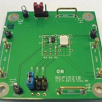
NCP1521UEVB
Manufacturer Part Number
NCP1521UEVB
Description
EVAL BOARD FOR NCP1521U
Manufacturer
ON Semiconductor
Specifications of NCP1521UEVB
Design Resources
NCP1521UEVB BOM NCP1521UEVB Schematic NCP1521UEVB Gerber Files
Main Purpose
DC/DC, Step Down
Outputs And Type
1, Non-Isolated
Voltage - Output
0.9 ~ 3.3 V
Current - Output
600mA
Voltage - Input
3.6V
Regulator Topology
Buck
Frequency - Switching
1.5MHz
Board Type
Fully Populated
Utilized Ic / Part
NCP1521
Lead Free Status / RoHS Status
Lead free / RoHS Compliant
Power - Output
-
Lead Free Status / Rohs Status
Lead free / RoHS Compliant
For Use With/related Products
NCP1521U
Other names
NCP1521UEVBOS


PCB Layout Recommendations
mode power conversion. Careful PCB layout can help to
minimize ground bounce, EMI noise and unwanted
feedback that can affect the performance of the converter.
Hints suggested below can be used as a guideline in most
situations.
Good PCB layout plays an important role in switching
1. Use star-ground connection to connect the IC
ground nodes and capacitor GND nodes together
at one point. Keep them as close as possible, and
then connect this to the ground plane through
several vias. This will reduce noise in the ground
plane by preventing the switching currents from
flowing through the ground plane.
VIN
CIN
OFF ON
Figure 25. NCP1521 Board Schematic
Figure 26. NCP1521 Board Layout
APPLICATION BOARD
1
2
3
http://onsemi.com
VIN
GND
EN
NCP1521
FB
12
LX
schematic, layout, and bill of materials:
5
4
The following shows the NCP1521 demo board
2. Place the power components (i.e., input capacitor,
3. Separate the feedback path of the output voltage
4. Place the DC-DC converter away from noise
COUT
inductor and output capacitor) as close together
as possible for best performance. All connecting
traces must be short, direct, and wide to reduce
voltage errors caused by resistive losses through
the traces.
from the power path. Keep this path close to the
NCP1521 circuit. And also route it away from
noisy components. This will prevent noise from
coupling into the voltage feedback trace.
sensitive circuitry, such as RF circuits.
L
R1
R2
VOUT
Cff
Related parts for NCP1521UEVB
Image
Part Number
Description
Manufacturer
Datasheet
Request
R

Part Number:
Description:
1.5 Mhz, 600 Ma, Highefficiency, Low Quiescent Current, Adjustable Output Voltage Stepdown Converter
Manufacturer:
ON Semiconductor
Datasheet:
Part Number:
Description:
ON Semiconductor [VOLTAGE REGULATOR]
Manufacturer:
ON Semiconductor
Datasheet:
Part Number:
Description:
357-036-542-201 CARDEDGE 36POS DL .156 BLK LOPRO
Manufacturer:
ON Semiconductor
Datasheet:
Part Number:
Description:
357-036-542-201 CARDEDGE 36POS DL .156 BLK LOPRO
Manufacturer:
ON Semiconductor
Datasheet:
Part Number:
Description:
357-036-542-201 CARDEDGE 36POS DL .156 BLK LOPRO
Manufacturer:
ON Semiconductor
Datasheet:
Part Number:
Description:
357-036-542-201 CARDEDGE 36POS DL .156 BLK LOPRO
Manufacturer:
ON Semiconductor
Datasheet:
Part Number:
Description:
357-036-542-201 CARDEDGE 36POS DL .156 BLK LOPRO
Manufacturer:
ON Semiconductor
Datasheet:
Part Number:
Description:
357-036-542-201 CARDEDGE 36POS DL .156 BLK LOPRO
Manufacturer:
ON Semiconductor
Datasheet:
Part Number:
Description:
357-036-542-201 CARDEDGE 36POS DL .156 BLK LOPRO
Manufacturer:
ON Semiconductor
Datasheet:
Part Number:
Description:
357-036-542-201 CARDEDGE 36POS DL .156 BLK LOPRO
Manufacturer:
ON Semiconductor
Datasheet:
Part Number:
Description:
357-036-542-201 CARDEDGE 36POS DL .156 BLK LOPRO
Manufacturer:
ON Semiconductor
Datasheet:
Part Number:
Description:
357-036-542-201 CARDEDGE 36POS DL .156 BLK LOPRO
Manufacturer:
ON Semiconductor
Datasheet:
Part Number:
Description:
Manufacturer:
ON Semiconductor
Datasheet:
Part Number:
Description:
Manufacturer:
ON Semiconductor
Datasheet: