NCP5602EVB ON Semiconductor, NCP5602EVB Datasheet - Page 3
NCP5602EVB
Manufacturer Part Number
NCP5602EVB
Description
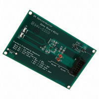
EVAL BOARD FOR NCP5602
Manufacturer
ON Semiconductor
Specifications of NCP5602EVB
Design Resources
NCP5602 EVB BOM NCP5602EVB Gerber Files NCP5602 EVB Schematic
Current - Output / Channel
60mA
Outputs And Type
2, Non-Isolated
Voltage - Output
4.8 ~ 5.7 V
Features
Dimmable
Voltage - Input
3.6V
Utilized Ic / Part
NCP5602
Core Chip
NCP5602
Topology
Charge Pump
No. Of Outputs
2
Development Tool Type
Hardware - Eval/Demo Board
Leaded Process Compatible
Yes
Mcu Supported Families
NCP5602
Rohs Compliant
Yes
Lead Free Status / RoHS Status
Lead free / RoHS Compliant
For Use With/related Products
NCP5602
Other names
NCP5602EVBOS


1. Using low ESR ceramic capacitor is mandatory to optimize the Charge Pump efficiency.
2. Total DC−DC output current is limited to 60 mA.
PIN FUNCTION DESCRIPTION
Pin No.
10
11
12
1
2
3
4
5
6
7
8
9
Symbol
VOUT
LED1
LED2
VBAT
GND
SDA
I
SCL
C2P
C2N
C1P
C1N
REF
OUTPUT, POWER
INPUT, ANALOG
INPUT, POWER
INPUT, POWER
INPUT, DIGITAL
INPUT, DIGITAL
INPUT, POWER
Function
POWER
POWER
POWER
POWER
POWER
http://onsemi.com
This pin is the GROUND signal for the analog and digital blocks and must be
connected to the system ground. This pin is the GROUND reference for the
DC−DC converter and the output current control. The pin must be connected
This pin sinks to ground and monitors the current flowing into the first LED,
intended to be used in backlight application. The current is limited to 30 mA
maximum (see Note 2). When the ICON bit of the LED−REG register is
High, the LED2 fulfills the ICON function. In this case, LED1 is deactivated.
This pin sinks to ground and monitors the current flowing into the second
LED, intended to be used in backlight application. The current is limited to
30 mA maximum (see Note 2). When the ICON bit of the LED−REG register
is High, the LED2 fulfills the ICON function. In this case, LED1 is
deactivated. The ICON current is 600 mA typical.
This pin provides the reference current, based on the internal bandgap
voltage reference, to control the output current flowing in the LED. A 1%
tolerance, or better, resistor shall be used to get the highest accuracy of the
LED biases. An external current source can be used to bias this pin to dim
the light coming out of the LED.
In no case shall the voltage at pin 4 be forced either higher or lower than the
600 mV provided by the internal reference.
This pin carries the data provided by the I2C protocol. The content of the
SDA byte is used to program the mode of operation and to set up the output
current (see Table 2).
This pin carries the I2C clock to control the DC−DC converter and to set up
the output current. The SCL clock is associated with the SDA signal.
This pin provides the output voltage supplied by the DC−DC converter. The
Vout pin must be bypassed by 1.0 mF ceramic capacitor located as close as
possible to the pin to properly bypass the output voltage to ground. The
circuit shall not operate without such bypass capacitor properly connected to
the Vout pin.
The output voltage is internally clamped to 5.5 V maximum in the event of no
load situation. On the other hand, the output current is limited to 40 mA
(typical) in the event of a short circuit to ground.
One side of the external charge pump capacitor (C
One side of the external charge pump capacitor (C
One side of the external charge pump capacitor (C
Input Battery voltage to supply the analog and digital blocks. The pin must be
decoupled to ground by a 1.0 mF ceramic capacitor.
One side of the external charge pump capacitor (C
to the system ground, a ground plane being strongly recommended.
pin, associated with C2N (see Note 1).
pin, associated with C2P (see Note 1).
pin, associated with C1N, pin 11 (see Note 1).
pin, associated with C1P, pin 10 (see Note 1).
3
Description
FLY
FLY
FLY
FLY
) is connected to this
) is connected to this
) is connected to this
) is connected to this
Related parts for NCP5602EVB
Image
Part Number
Description
Manufacturer
Datasheet
Request
R

Part Number:
Description:
High Efficiency Ultra Small Thinnest White LED Driver
Manufacturer:
ON Semiconductor
Datasheet:
Part Number:
Description:
ON Semiconductor [VOLTAGE REGULATOR]
Manufacturer:
ON Semiconductor
Datasheet:
Part Number:
Description:
357-036-542-201 CARDEDGE 36POS DL .156 BLK LOPRO
Manufacturer:
ON Semiconductor
Datasheet:
Part Number:
Description:
357-036-542-201 CARDEDGE 36POS DL .156 BLK LOPRO
Manufacturer:
ON Semiconductor
Datasheet:
Part Number:
Description:
357-036-542-201 CARDEDGE 36POS DL .156 BLK LOPRO
Manufacturer:
ON Semiconductor
Datasheet:
Part Number:
Description:
357-036-542-201 CARDEDGE 36POS DL .156 BLK LOPRO
Manufacturer:
ON Semiconductor
Datasheet:
Part Number:
Description:
357-036-542-201 CARDEDGE 36POS DL .156 BLK LOPRO
Manufacturer:
ON Semiconductor
Datasheet:
Part Number:
Description:
357-036-542-201 CARDEDGE 36POS DL .156 BLK LOPRO
Manufacturer:
ON Semiconductor
Datasheet:
Part Number:
Description:
357-036-542-201 CARDEDGE 36POS DL .156 BLK LOPRO
Manufacturer:
ON Semiconductor
Datasheet:
Part Number:
Description:
357-036-542-201 CARDEDGE 36POS DL .156 BLK LOPRO
Manufacturer:
ON Semiconductor
Datasheet:
Part Number:
Description:
357-036-542-201 CARDEDGE 36POS DL .156 BLK LOPRO
Manufacturer:
ON Semiconductor
Datasheet:
Part Number:
Description:
357-036-542-201 CARDEDGE 36POS DL .156 BLK LOPRO
Manufacturer:
ON Semiconductor
Datasheet:
Part Number:
Description:
Manufacturer:
ON Semiconductor
Datasheet:
Part Number:
Description:
Manufacturer:
ON Semiconductor
Datasheet: