NCP3065SOBSTGEVB ON Semiconductor, NCP3065SOBSTGEVB Datasheet
NCP3065SOBSTGEVB
Specifications of NCP3065SOBSTGEVB


Related parts for NCP3065SOBSTGEVB


NCP3065SOBSTGEVB Summary of contents
Page 1
NCP3065, NCV3065 Up to 1.5 A Constant Current Switching Regulator for LEDs The NCP3065 is a monolithic switching regulator designed to deliver constant current for powering high brightness LEDs. The device has a very low feedback voltage of 235 mV ...
Page 2
Switch Collector Switch Emitter 2 Timing Capacitor 3 GND 4 (Top View) Figure 2. Pin Connections 8 N.C. COMPARATOR 7 I Sense Comparator Inverting Input PIN DESCRIPTION Pin No. Pin Name 1 Switch Collector ...
Page 3
MAXIMUM RATINGS (measured vs. pin 4, unless otherwise noted) Rating V (Pin 6) CC Comparator Inverting Input (Pin 5) Darlington Switch Collector (Pin 1) Darlington Switch Emitter (Pin 2) (Transistor OFF) Darlington Switch Collector to Emitter (Pins 1−2) Darlington Switch ...
Page 4
ELECTRICAL CHARACTERISTICS Characteristic OSCILLATOR Frequency Discharge to Charge Current Ratio Capacitor Discharging Current Capacitor Charging Current Current Limit Sense Voltage OUTPUT SWITCH (Note 5) Darlington Switch Collector to Emitter Voltage Drop Collector Off−State Current COMPARATOR Threshold Voltage Threshold Voltage Line ...
Page 5
Ct, CAPACITANCE (nF) Figure 5. Oscillator Frequency vs. Oscillator Timing Capacitor 2.4 2.2 ...
Page 6
T , JUNCTION TEMPERATURE (°C) J Figure 11. Comparator Threshold Voltage vs. Temperature 6.0 5.5 5.0 4.5 4.0 3.5 3.0 2.5 2.0 3.0 Figure 13. Standby ...
Page 7
The NCP3065 is a monolithic power switching regulator optimized for LED Driver applications. Its flexible architecture enables the system designer to directly implement a step−up or step−down topology with a minimum number of external components for driving LEDs. A representative ...
Page 8
Peak Current Sense Comparator Under normal conditions, the output switch conduction is initiated by the Voltage Feedback comparator and terminated by the oscillator. Abnormal operating conditions occur when the converter output is overloaded or when feedback voltage sensing is lost. ...
Page 9
Figures 16 through 24 show the simplicity and flexibility of the NCP3065. Two main converter topologies are demonstrated with actual test data shown below each of the circuit diagrams. (See Notes off V in ...
Page 10
1206 1206 1206 1206 1206 1206 1206 1 +VIN 0.1 mF 220 GND J4 1 BC807−LT1G +VAUX ...
Page 11
Figure 18. 1.5 A Buck Demoboard Layout 7.2 V, Output Cap 100 mF OUT 3.6 V, Output Cap 100 mF OUT ...
Page 12
+VIN C3 J4 0.1 mF 220 GND J6 BC807−LT1G BC817−LT1G 1 +VAUX R10 1 1k2 ON/OFF J7 R10 ...
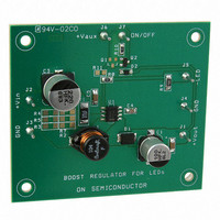
Page 13
Figure 23. Boost Demoboard Layout INPUT VOLTAGE (V) IN Figure 24. Efficiency vs. Input Voltage for the Boost Demo Board ...
Page 14
1206 1206 1206 1206 1206 1206 1 +VIN 0.1 mF 220 GND J4 BC807−LT1G ...
Page 15
Figure 26 Buck Demoboard Layout ORDERING INFORMATION Device NCP3065MNTXG NCP3065PG NCP3065DR2G NCV3065MNTXG NCV3065PG NCV3065DR2G †For information on tape and reel specifications, including part orientation and tape sizes, please refer to our Tape and Reel Packaging Specifications Brochure, BRD8011/D. ...
Page 16
F −A− NOTE 2 C −T− N SEATING PLANE 0.13 (0.005) M PACKAGE DIMENSIONS 8 LEAD PDIP CASE 626−05 ISSUE http://onsemi.com 16 ...
Page 17
... G C SEATING PLANE −Z− 0.25 (0.010 *For additional information on our Pb−Free strategy and soldering details, please download the ON Semiconductor Soldering and Mounting Techniques Reference Manual, SOLDERRM/D. PACKAGE DIMENSIONS SOIC−8 NB CASE 751−07 ISSUE 0.10 (0.004 SOLDERING FOOTPRINT* 1 ...
Page 18
... NOTE 3 0.05 C *For additional information on our Pb−Free strategy and soldering details, please download the ON Semiconductor Soldering and Mounting Techniques Reference Manual, SOLDERRM/D. N. American Technical Support: 800−282−9855 Toll Free USA/Canada Europe, Middle East and Africa Technical Support: Phone: 421 33 790 2910 Japan Customer Focus Center Phone: 81− ...